Method and pad for polishing wafer
a technology of polishing pad and wafer, which is applied in the direction of flexible wheel, manufacturing tools, lapping machines, etc., can solve the problems of deterioration of the flatness of the wafer, the influence of precision in the polishing apparatus, and the inability to absorb vibration in processing, etc., to achieve the effect of effectively preventing a sag
- Summary
- Abstract
- Description
- Claims
- Application Information
AI Technical Summary
Benefits of technology
Problems solved by technology
Method used
Image

Examples
experimental example 1
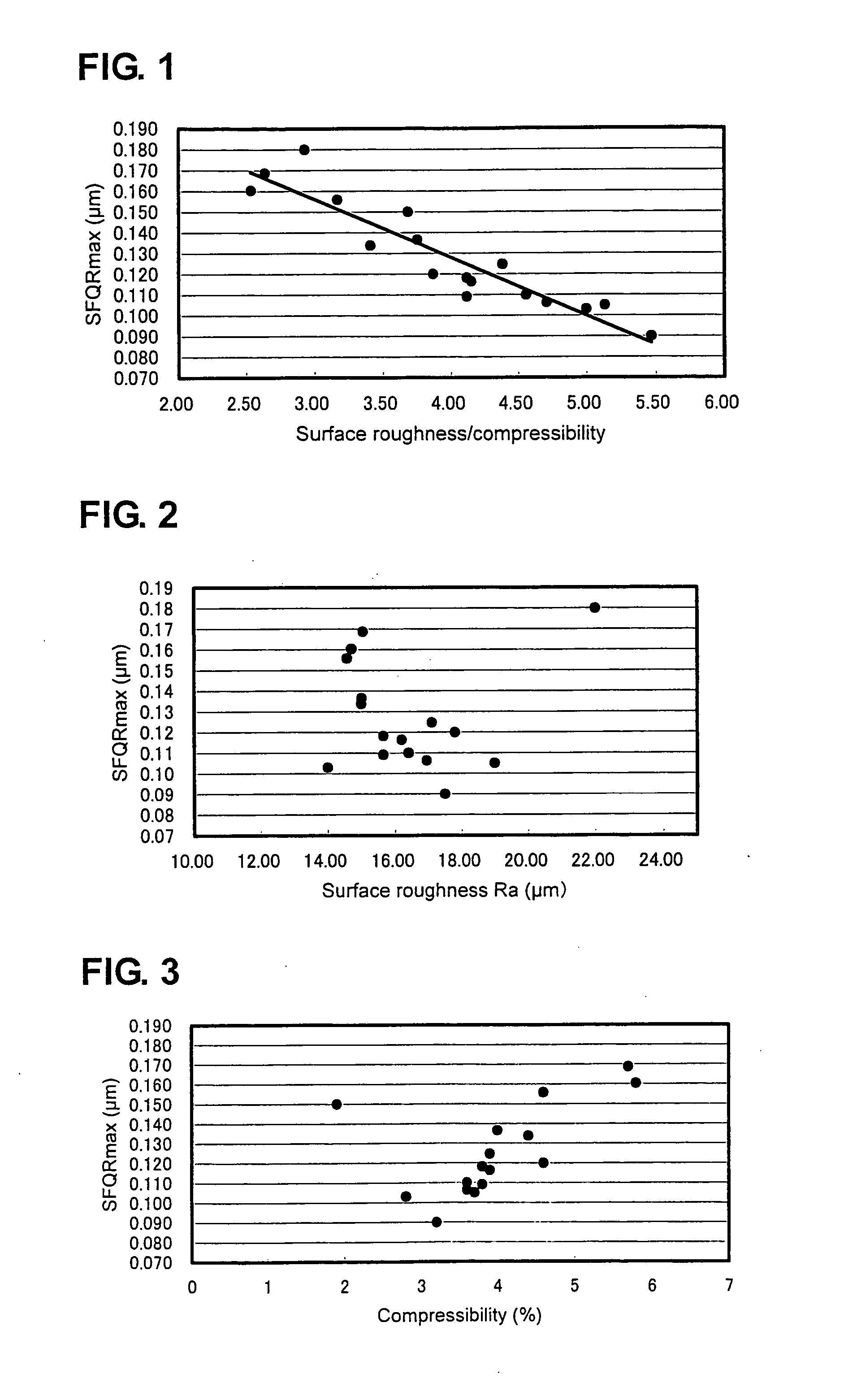
[0035] A ratio of {surface roughness (μm) / compressibility (%)} of a polishing pad was changed to investigate a relationship between the ratio and wafer flatness after polishing. Using a flatness tester 9700 E+ made by ADE Corporation, flatness was measured in terms of SFQR (Site Front least sQuares Range: difference of undulation in each site on a wafer surface) excluding an outer peripheral portion of 2 mm with a size of 25 mm square cell, and the max value of the cells on the wafer surface (SFQRmax) was evaluated.
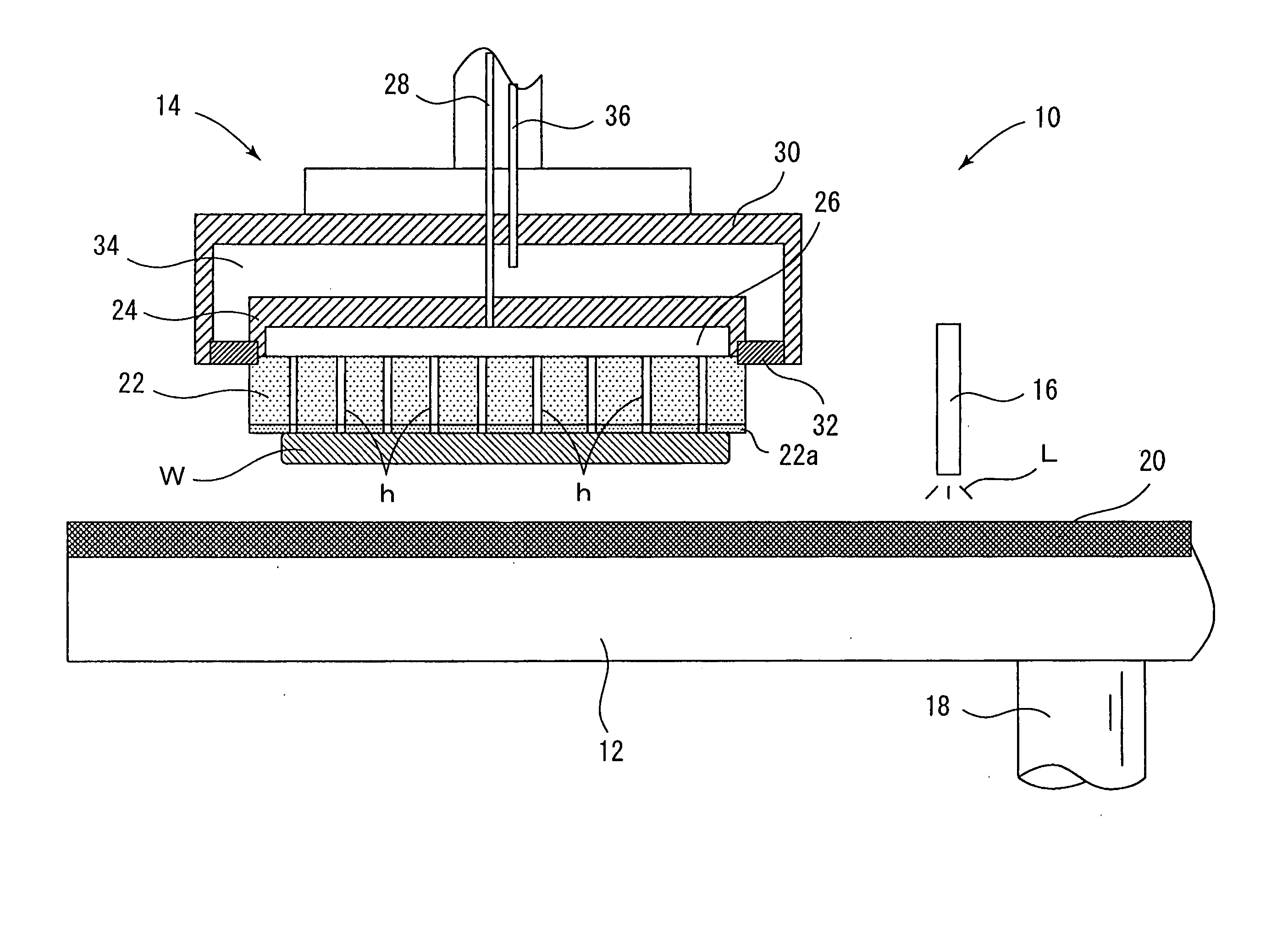
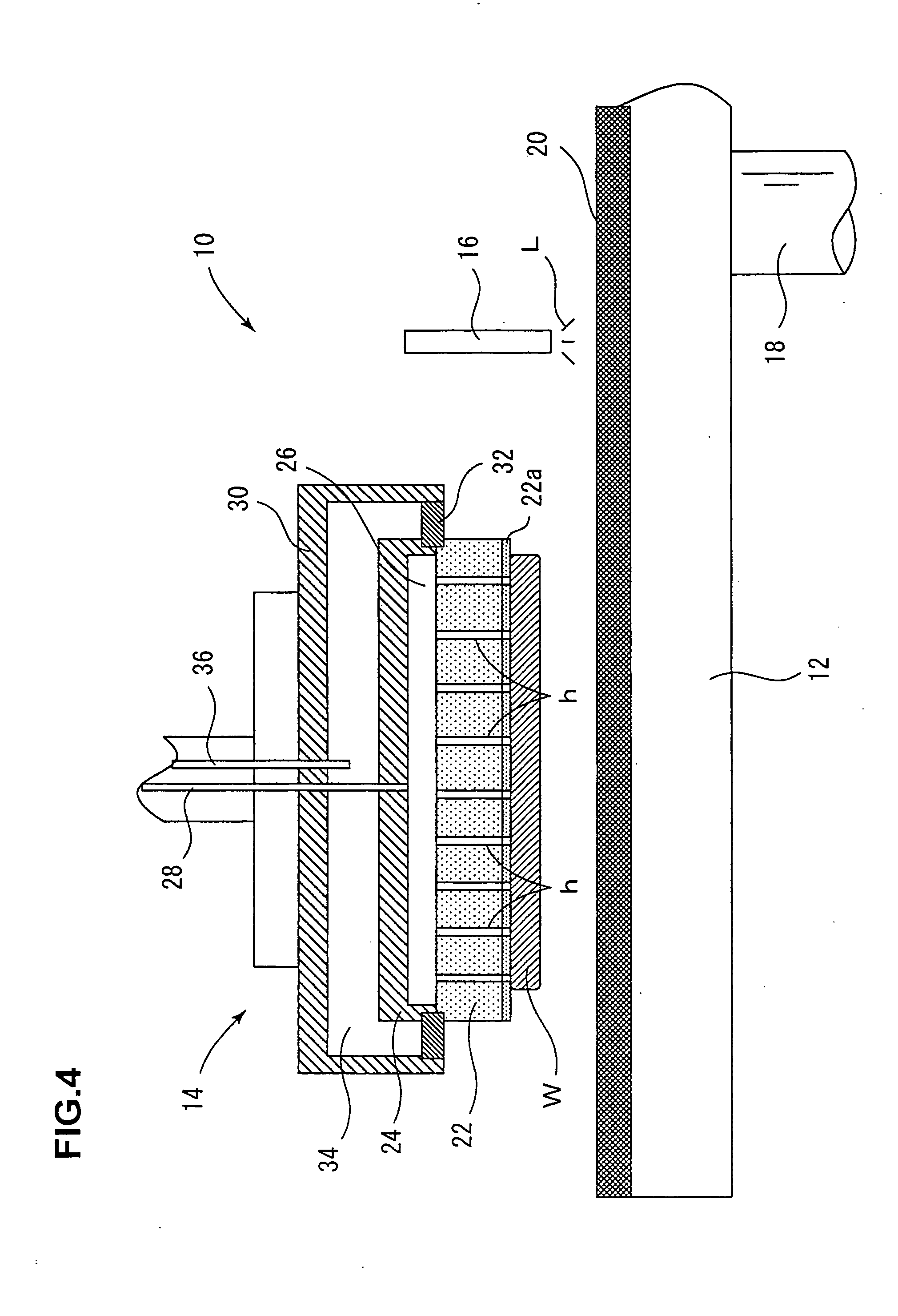
[0036] With a polishing apparatus similar to the polishing apparatus shown in FIG. 4 in which there were used various polishing pads adhered thereon each having a different ratio value of {surface roughness (μm) / compressibility (%)}, 8-inch silicon wafers subjected to etching treatment were polished using abrasive slurry containing colloidal silica (at a pH value of 10.5) under polishing conditions of a polishing pressure of 300 g / cm2 and a polishing time of 15 min.
[00...
example 1
[0040] Using a polishing apparatus similar to the polishing apparatus shown in FIG. 4 having a polishing pad with the compressibility of 3.9% and the surface roughness of 16.2 μm ({surface roughness (μm) / compressibility (%)} =4.15), one hundred pieces of 8-inch silicon wafers were polished. Flatness values of the polished wafers were measured under tight conditions excluding outer peripheral portions of 3 mm and 2 mm.
[0041] As a result of polishing, flatness values of all the polished wafers were SFQRmax=0.12 μm or less. Even when evaluation was performed on a wafer surface excluding the outer peripheral portion of 2 mm, flatness values were SFQRmax=0.12 μm or less; it is found that the wafers are stably polished to be flat up to the outer peripheral portion.
example 2
[0042] Using a polishing apparatus similar to the polishing apparatus shown in FIG. 4 having a polishing pad with the compressibility of 4.6% and the surface roughness of 17.8 μm ({surface roughness (μm) / compressibility (%)} =3.87), one hundred pieces of 8-inch silicon wafers were polished. Flatness values of the polished wafers were measured under tight conditions excluding outer peripheral portions of 3 mm and 2 mm.
[0043] As a result of polishing, flatness values of all the polished wafers were SFQRmax=0.13 μm or less. Even when evaluation was performed on a wafer surface excluding the outer peripheral portion of 2 mm, flatness values were SFQRmax=0.13 μm or less; it is found that the wafers are stably polished to be flat up to the outer peripheral portion.
PUM
| Property | Measurement | Unit |
|---|---|---|
| surface roughness | aaaaa | aaaaa |
| flatness | aaaaa | aaaaa |
| length | aaaaa | aaaaa |
Abstract
Description
Claims
Application Information
 - R&D
- Intellectual Property
- Life Sciences
- Materials
- Tech Scout
- Unparalleled Data Quality
- Higher Quality Content
- 60% Fewer Hallucinations
Browse by: Latest US Patents, China's latest patents, Technical Efficacy Thesaurus, Application Domain, Technology Topic, Popular Technical Reports.
© 2025 PatSnap. All rights reserved.Legal|Privacy policy|Modern Slavery Act Transparency Statement|Sitemap|About US| Contact US: help@patsnap.com