Connection structure of circuit substrate

a technology of connecting structure and substrate, which is applied in the direction of coupling device connection, packaging goods type, transportation and packaging, etc., can solve the problems of reel-to-reel process deformation or other damage to the connected portion, easy humidity damage to the ics, etc., to improve the tensile strength of the connected substrate, prevent deformation or damage at the connected portion, and improve the connection structure

Inactive Publication Date: 2005-01-27
SAMSUNG ELECTRONICS CO LTD
View PDF2 Cites 17 Cited by
  • Summary
  • Abstract
  • Description
  • Claims
  • Application Information

AI Technical Summary

Benefits of technology

[0011] The present invention is directed to an improved connection structure for a circuit substrate, improving the tensile strength of the connected substrates, thus preventing deformation or damage at the connected portion.

Problems solved by technology

Furthermore, ICs damage easily by humidity, shock or thermal stress.
The reel-to-reel process occasionally deforms or otherwise damages the connected portion 40.

Method used


Image

  • Connection structure of circuit substrate
  • Connection structure of circuit substrate
  • Connection structure of circuit substrate

Examples


Embodiment Construction

[0023] Exemplary embodiments of the present invention will be described below with reference to the accompanying drawings.

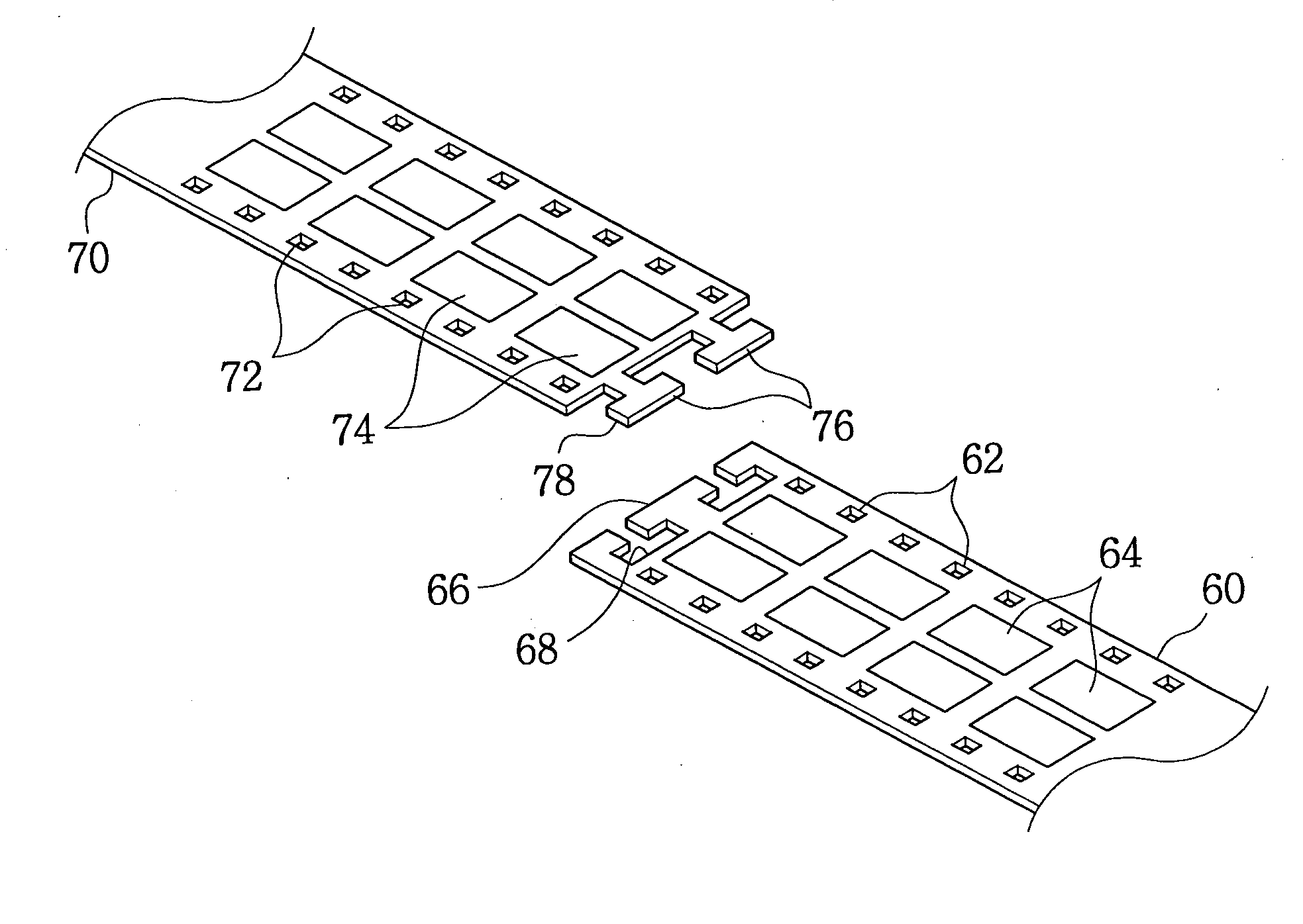
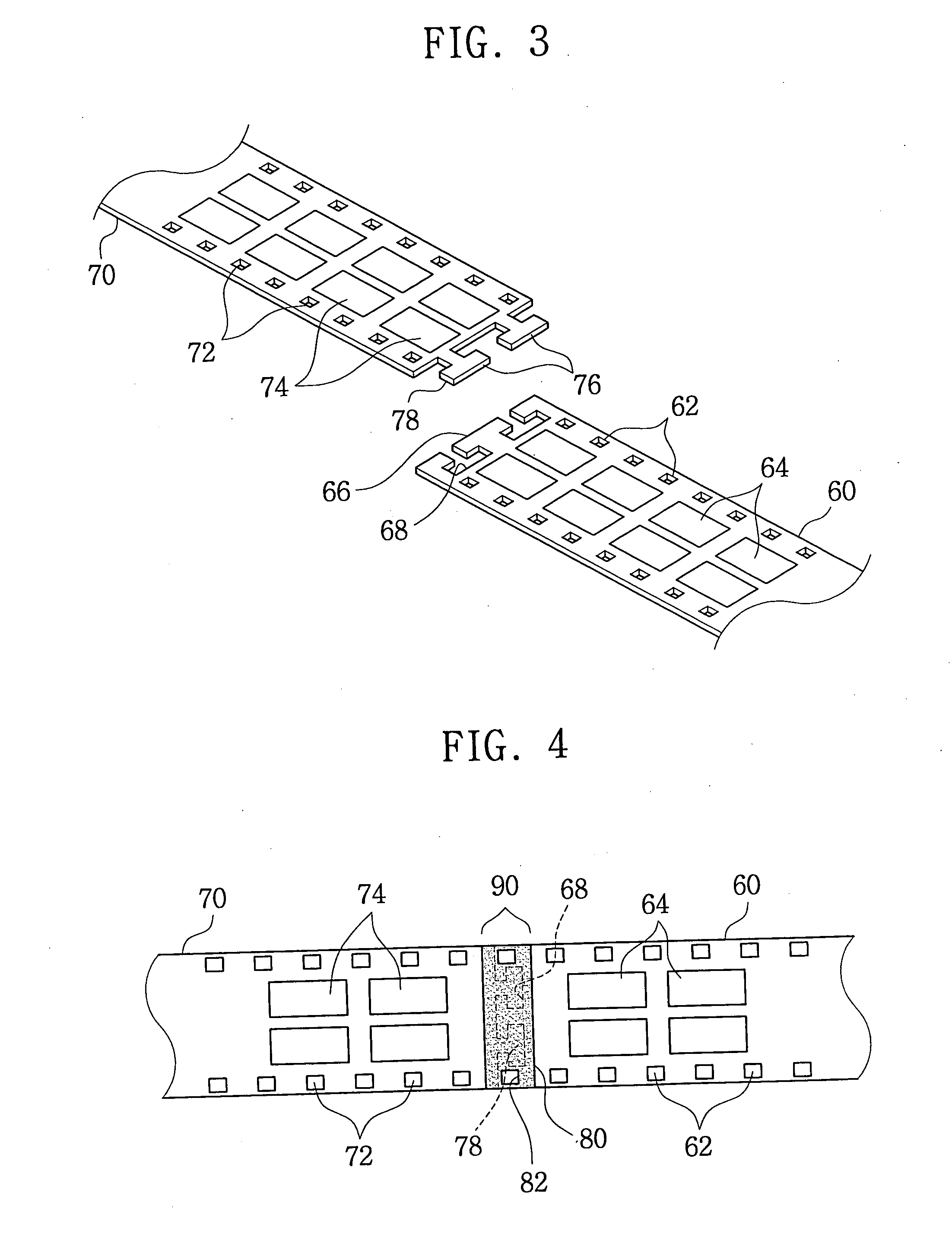
[0024]FIG. 3 is an exploded perspective view illustrating a connection for circuit substrates in accordance with an embodiment of the present invention. FIG. 4 is a plan view of a connection structure shown in FIG. 3.

[0025] Referring to FIGS. 3 and 4, circuit substrates are connected in accordance with a T shaped embodiment of the present invention. The rear end 68 of a first circuit substrate 60 may be connected to the front end 76 of a second circuit substrate 70. An adhesive tape 80 may attach the connected ends of the first and second circuit substrates 60 and 70, thus securing the connected portion 90. Therefore, the connection structure geometry provides bonding strength for the connection structure in addition to the adhesive tape 80. This connection structure of circuit substrates improves bonding strength in comparison to conventional connection struct...


PUM

PropertyMeasurementUnit
thickaaaaaaaaaa
connection structureaaaaaaaaaa
shapeaaaaaaaaaa

Abstract

The present invention provides an improved connection for circuit substrates. The circuit substrates are connected at concave and convex portions at their ends. The concave portion is formed such that the inside width is larger than the entrance width. The convex portion fits into the concave portion. Thereby, a connected portion of the circuit substrates has increased tensile strength. Furthermore, abnormality of the connected portion of the circuit substrates may be easily perceived.

Description

CROSS REFERENCE TO RELATED APPLICATIONS [0001] This U.S. non-provisional application claims priority from Korean Patent Application No. 2003-50203 filed Jul. 22, 2003, the contents of which are incorporated by reference in their entirety. BACKGROUND OF THE INVENTION [0002] 1. Field of the Invention [0003] The present invention relates to semiconductor packages and, more particularly, to a connection structure for connecting circuit substrates. [0004] 2. Description of the Related Art [0005] Integrated circuits (IC) have specific needs. Functionally, they require signal and power supplies. ICs can operate at high temperature and require heat dissipation. Furthermore, ICs damage easily by humidity, shock or thermal stress. Proper packaging satisfies these requirements. [0006] In semiconductor package fabrication, circuit substrates or package substrates may use lead frames, printed circuit boards, ceramic substrates or tape wiring substrates. Strip-type circuit substrates may be used ...

Claims


Application Information

Patent Timeline
Patent Type & Authority Applications(United States)
IPC IPC(8): H01L21/60B65D85/30H01L23/13H05K1/00H05K1/14H05K3/00
CPCH01L23/13H01L2924/15162H05K1/0393H05K1/142H05K3/0097H05K2201/10598Y10T29/49128H05K2203/1545H01L2924/0002H05K2201/209Y10T29/4913H01L2924/00H01L21/60
Inventor CHO, SUNG-DAELEE, JOO-HYUNG
Owner SAMSUNG ELECTRONICS CO LTD
Why Eureka
Try Eureka