Semiconductor device and method of manufacturing the same, circuit board, and electronic instrument

a semiconductor and semiconductor chip technology, applied in the direction of semiconductor devices, semiconductor/solid-state device details, electrical apparatus, etc., can solve the problem of insufficient measures to prevent the occurrence of short circuits between the upper and lower adjacent semiconductor chips

Active Publication Date: 2005-01-27
ADVANCED INTERCONNECT SYST LTD
View PDF9 Cites 90 Cited by
  • Summary
  • Abstract
  • Description
  • Claims
  • Application Information

AI Technical Summary

Problems solved by technology

In a conventional structure, a measure to prevent occurrence of short circui

Method used


Image

  • Semiconductor device and method of manufacturing the same, circuit board, and electronic instrument
  • Semiconductor device and method of manufacturing the same, circuit board, and electronic instrument
  • Semiconductor device and method of manufacturing the same, circuit board, and electronic instrument

Examples


Embodiment Construction

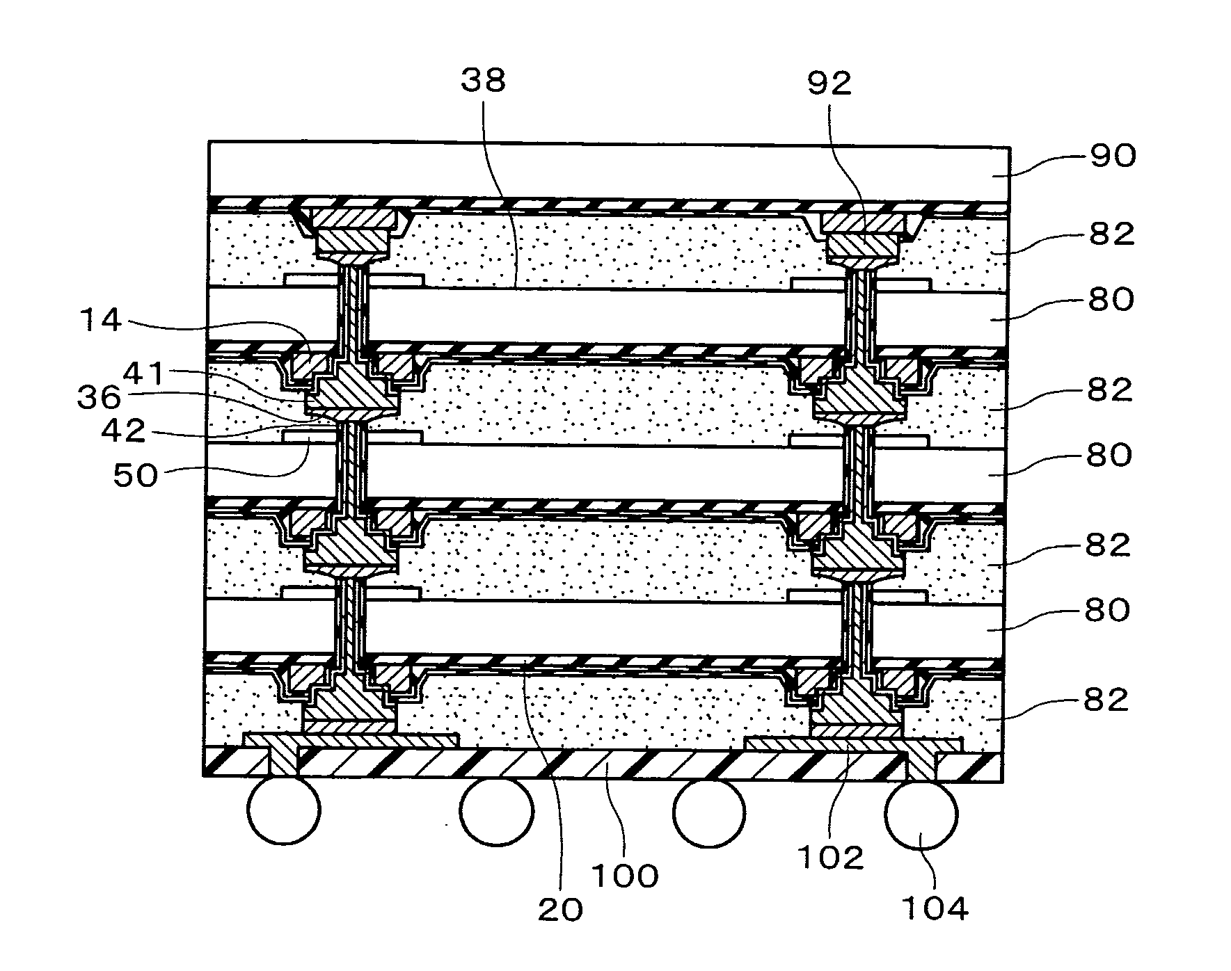
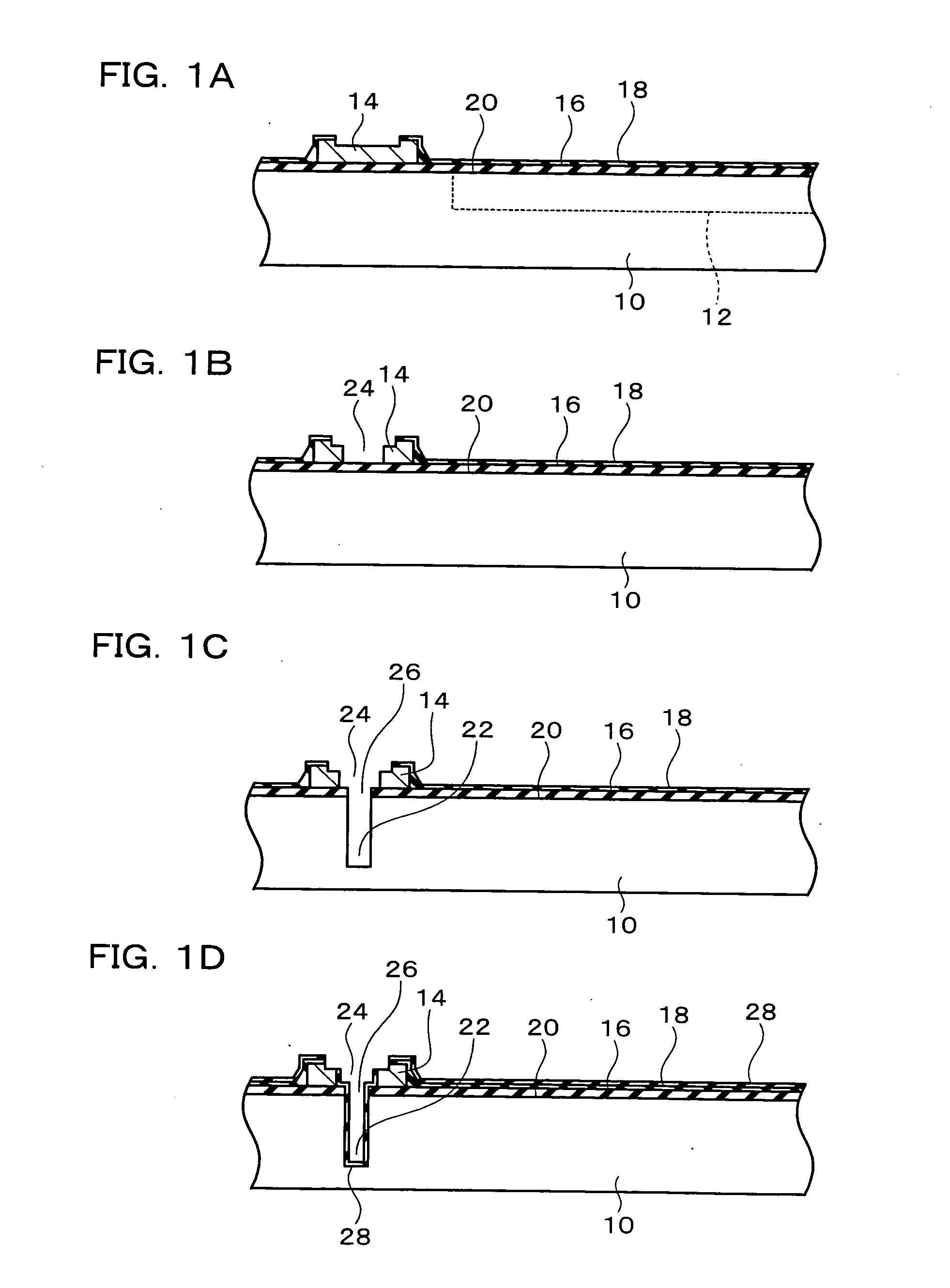
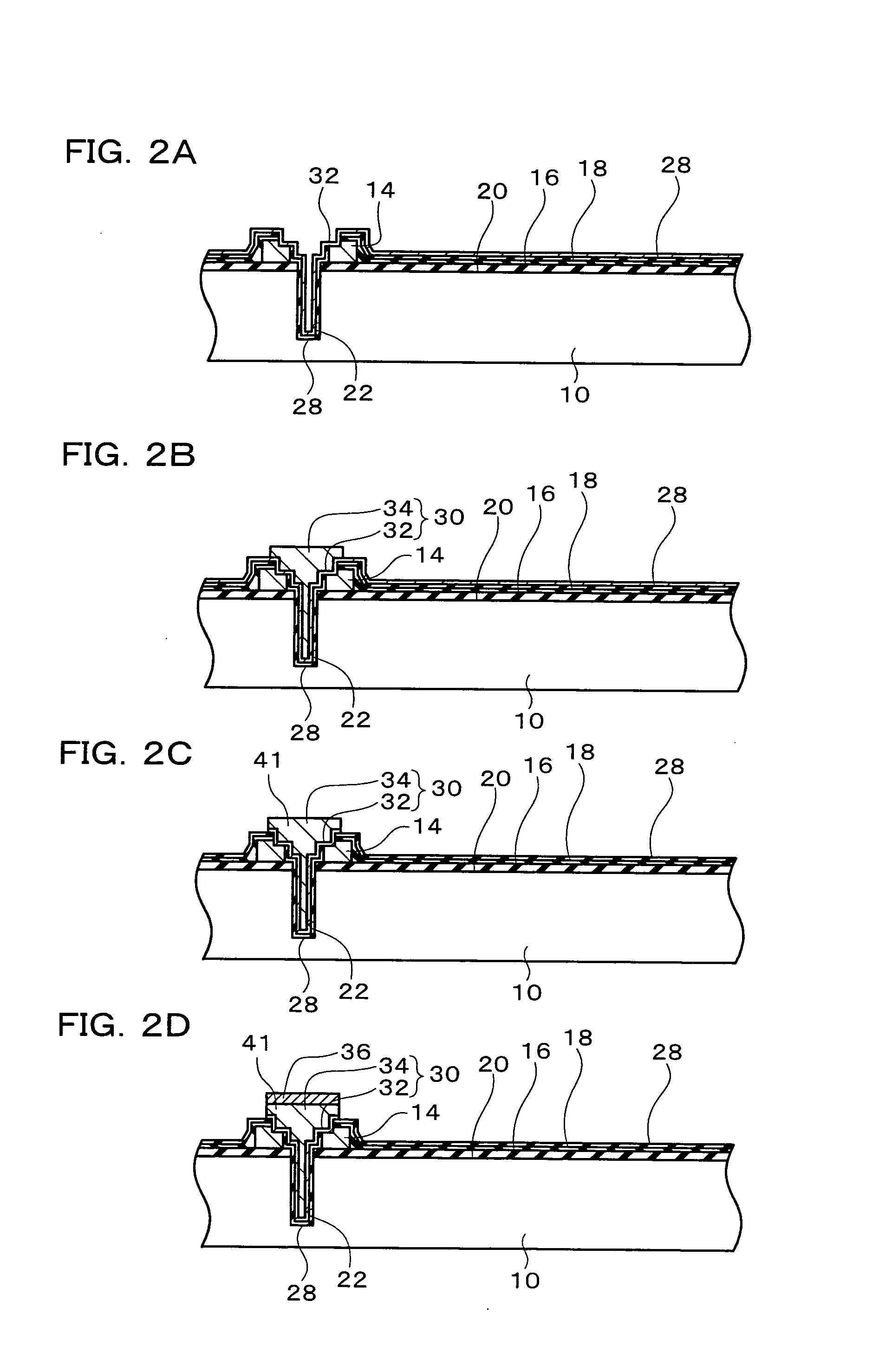
[0030] According to embodiments of the present invention, occurrence of short circuits between stacked semiconductor substrates can be prevented, and flowing property of an underfill can be increased.

[0031] (1) A semiconductor device according to one embodiment of the present invention includes:

[0032] a semiconductor substrate which includes a first surface in which an integrated circuit is formed, and a second surface opposite to the first surface;

[0033] a through-hole electrode which is formed through the semiconductor substrate, and includes a first projecting section which projects from the first surface and a second projecting section which projects from the second surface; and

[0034] an insulating layer which is formed in a region around the second projecting section except a part of the second surface so as to extend outward beyond an outer edge of the first projecting section.

[0035] According to this embodiment of the present invention, since the insulating layer is form...


PUM


Abstract

A semiconductor device includes a semiconductor substrate in which an integrated circuit is formed, a through-hole electrode which is formed through first and second surfaces of the semiconductor substrate and includes a first projecting section which projects from the first surface and a second projecting section which projects from the second surface, and an insulating layer which is formed in a region around the second projecting section except a part of the second surface so as to extend outward beyond an outer edge of the first projecting section.

Description

[0001] Japanese Patent Application No. 2003-175322, filed on Jun. 19, 2003, is hereby incorporated by reference in its entirety. BACKGROUND OF THE INVENTION [0002] The present invention relates to a semiconductor device and a method of manufacturing the same, a circuit board, and an electronic instrument. [0003] A semiconductor device in three-dimensional mounting form has been developed. It is known in the art that through-hole electrodes are formed in semiconductor chips, and the upper and lower through-hole electrodes are bonded by stacking the semiconductor chips. In a conventional structure, a measure to prevent occurrence of short circuits between the upper and lower adjacent semiconductor chips is insufficient. In more detail, solder used for electrical bonding melts and flows toward the periphery of the through-hole electrode, whereby short circuits with the semiconductor section occur in the terminal peripheral section. BRIEF SUMMARY OF THE INVENTION [0004] A semiconductor ...

Claims


Application Information

Patent Timeline
IPC IPC(8): H01L23/48H01L25/065H01L25/18H01L25/07
CPCH01L23/481H01L25/0657H01L2224/16H01L2924/15311H01L2225/06541H01L2924/01004H01L2924/01078H01L2225/06513H01L2224/13009H01L2224/05009H01L2224/05548H01L2224/05001H01L2224/05147H01L2224/05184H01L24/05H01L2924/00014
Inventor FUKAZAWA, MOTOHIKO
Owner ADVANCED INTERCONNECT SYST LTD
Why Eureka
Try Eureka