Monolithic ceramic electronic component and method for manufacturing monolithic ceramic electronic component

a technology of monolithic ceramic and electronic components, applied in the direction of variable capacitors, fixed capacitor details, fixed capacitors, etc., can solve the problems of serious affecting the impedance of the inductor, reducing the dielectric constant of ferrite by 14 to 13 or less, and deteriorating the strength and reliability of the outer electrodes, etc., to achieve low leakage flux and low cost

Active Publication Date: 2005-01-27
MURATA MFG CO LTD
View PDF2 Cites 22 Cited by
  • Summary
  • Abstract
  • Description
  • Claims
  • Application Information

AI Technical Summary

Benefits of technology

To overcome the problems described above, preferred embodiments of the present invention provide a monolithic ceramic electronic component in which the strength and reliability of the outer electrodes do not deteriorate and leakage flux is low, and also provide a method for manufacturing such a novel monolithic ceramic electronic component.

Problems solved by technology

However, in an inductor for high-frequency operation, stray capacitance in parallel with the inductor seriously affects the impedance of the inductor.
In particular, at GHz frequencies, small stray capacitance on the order of 0.01 pF to 0.1 pF seriously affects the impedance.
Unfortunately, decreasing the dielectric constant ε of ferrite by, for example, 14 to 13 or less is difficult practically because of the structure of ferrite.
As a result, the outer electrodes subside causing deterioration of the mechanical strength and the electrical connection reliability of the outer electrodes.
Consequently, when the sintered ferrite includes a coil element, leakage flux increases, and thus, high impedance cannot be achieved.

Method used


Image

  • Monolithic ceramic electronic component and method for manufacturing monolithic ceramic electronic component
  • Monolithic ceramic electronic component and method for manufacturing monolithic ceramic electronic component
  • Monolithic ceramic electronic component and method for manufacturing monolithic ceramic electronic component

Examples


Embodiment Construction

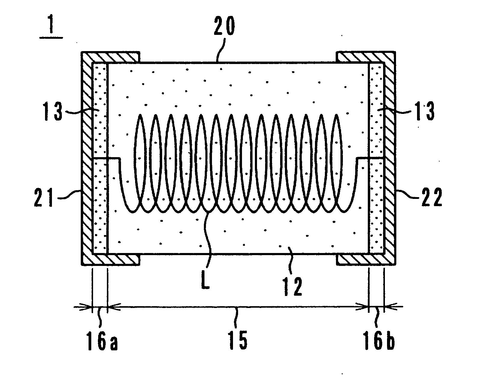
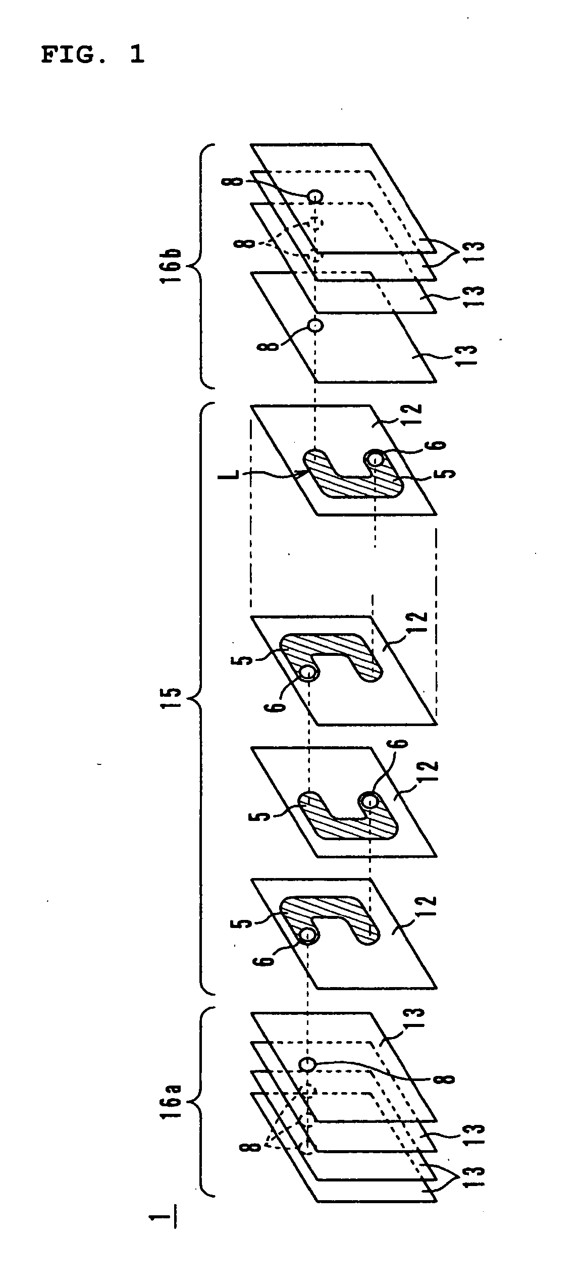
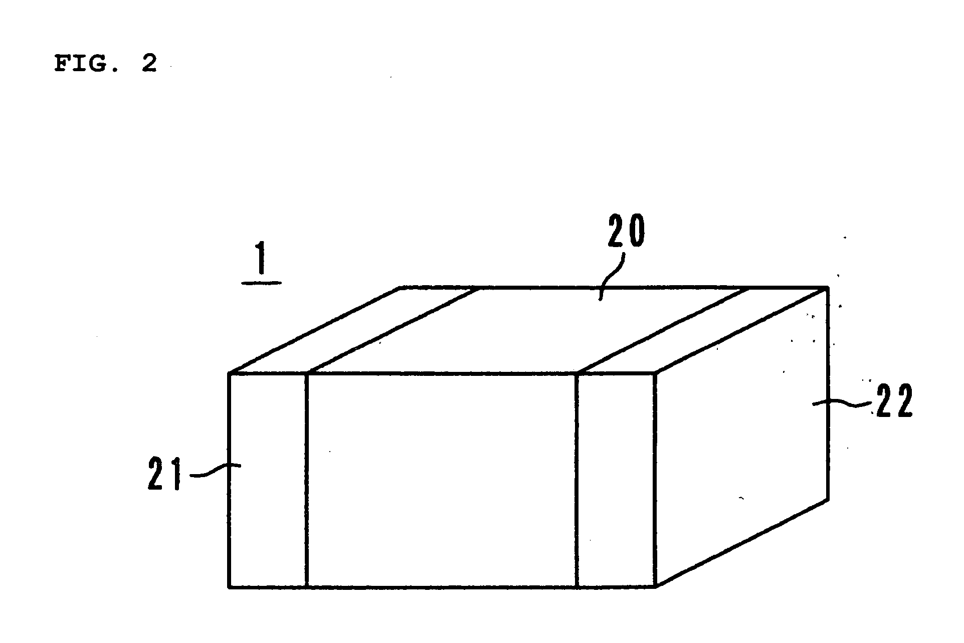
Preferred embodiments of the present invention including a monolithic ceramic electronic component and a method for manufacturing a monolithic ceramic electronic component will now be described below with reference to the drawings. In a first preferred embodiment, a monolithic inductor will be described as an example of the monolithic ceramic electronic component, however, the present invention is not limited thereto.

As shown in FIG. 1, a monolithic inductor I includes ceramic green sheets 12 for forming inner layers and ceramic green sheets 13 for forming outer layers, each of the ceramic green sheets 12 providing a via hole 6 for interlayer connection and a conductive pattern 5 for forming a coil, each of the ceramic green sheets 13 providing a lead via hole 8.

The ceramic green sheets 13 for forming the outer layers are preferably prepared by the following process: Nickel oxide, zinc oxide, and copper oxide are mixed and calcined at a temperature of about 800° C. for an hour,...


PUM

PropertyMeasurementUnit
particle sizeaaaaaaaaaa
diameteraaaaaaaaaa

Abstract

A monolithic ceramic component includes a coil-including region formed by stacking ceramic green sheets for defining inner layers having a porosity of about 30% to about 80%, and outer layer regions formed by stacking ceramic green sheets for defining outer layers have a porosity of about 10% or less. Outer electrodes are provided on the right end surface and the left end surface of a sintered ceramic laminate. That is, the outer electrodes are provided on the main surfaces of outermost ceramic sheets for outer layers.

Description

BACKGROUND OF THE INVENTION 1. Field of the Invention The present invention relates to monolithic ceramic electronic components, and more particularly, the present invention relates to monolithic ceramic electronic components such as monolithic inductors, monolithic capacitors, and LC combined monolithic components, and a method for manufacturing such a monolithic ceramic electronic component. 2. Description of the Related Art In recent years, electronic devices operating at high frequencies have become common. Inductors, LC combined components, LR combined components, LCR combined components, and the like, which can operate at gigahertz (GHz) frequencies, are required. However, in an inductor for high-frequency operation, stray capacitance in parallel with the inductor seriously affects the impedance of the inductor. In particular, at GHz frequencies, small stray capacitance on the order of 0.01 pF to 0.1 pF seriously affects the impedance. Consequently, to achieve a desired c...

Claims


Application Information

Patent Timeline
Patent Type & Authority Applications(United States)
IPC IPC(8): H01F17/00H01G4/12H01G4/30
CPCH01F17/0013Y10T29/43H01G4/30
Inventor TAKAZAWA, TOMOO
Owner MURATA MFG CO LTD
Why Eureka
Try Eureka