

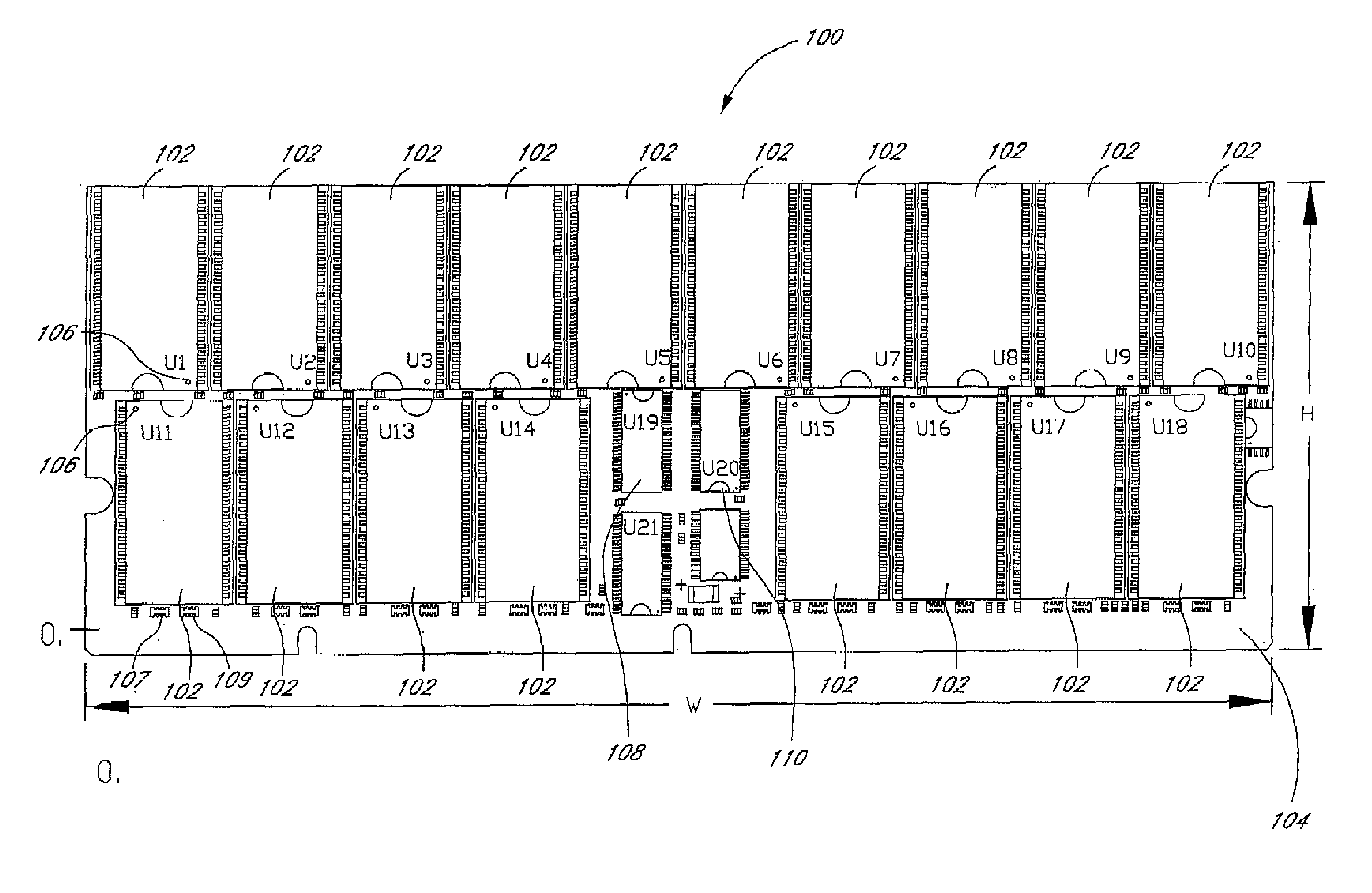
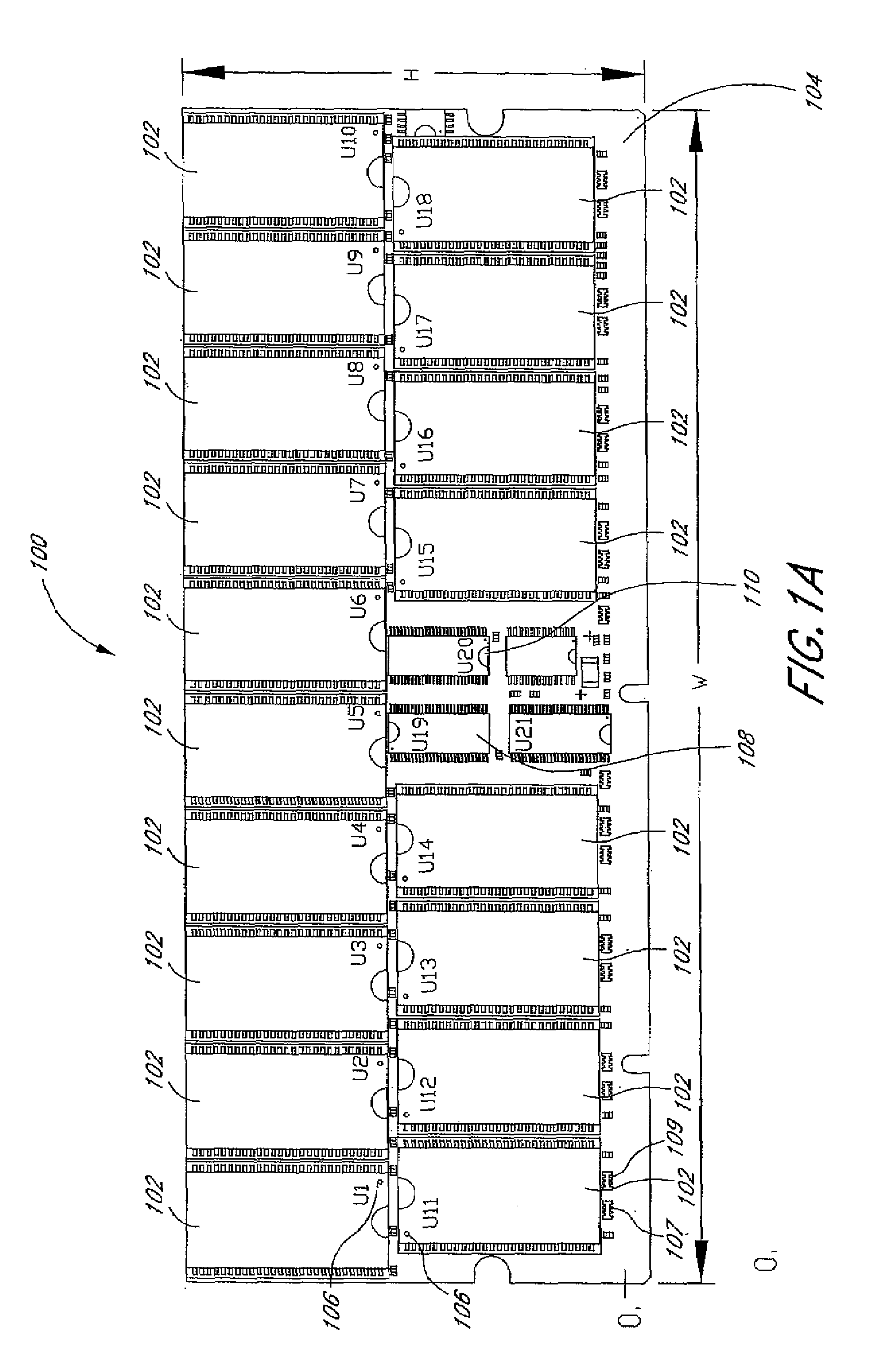
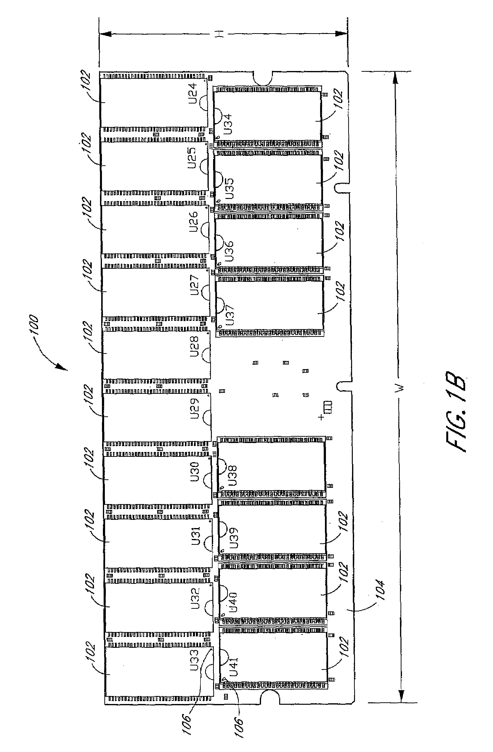
Arrangement of integrated circuits in a memory module
a memory module and integrated circuit technology, applied in the field of memory modules, can solve the problems of high heat generation, corresponding increase in surface area, and memory modules using stacked integrated circuits have substantial disadvantages over memory modules using a single layer of integrated circuits
- Summary
- Abstract
- Description
- Claims
- Application Information
AI Technical Summary
Benefits of technology
Problems solved by technology
Method used
Image

Examples
Embodiment Construction
Cross Reference to Related Applications
[0001] This application is a continuation-in-part of U.S. Patent Application No. 10 / 094,512, filed March 7, 2002, the disclosure of which is incorporated in its entirety by reference herein. This application also claims priority to U.S. Provisional Patent No. 60 / 516,684, filed November 3, 2003, the disclosure of which is incorporated in its entirety by reference herein. This application is related to the following co-pending applications: U.S. Patent Application No. 10 / 674,240, filed September 29, 2003; U.S. Patent Application No. 10 / 674,082, filed September 29, 2003; U.S. Patent Application No. 10 / 765,488 filed on January 27, 2004; and U.S. Patent Application No. 10 / 765,420 filed on January 27, 2004. Each of these co-pending applications is a divisional of U.S. Patent Application No. 10 / 094,512, filed March 7, 2002, and each of these co-pending applications is incorporated in its entirety by reference herein. This application is also relat...
PUM
 Abstract
Description
Claims
Application Information