Liquid crystal display device

a display device and liquid crystal technology, applied in semiconductor devices, instruments, computing, etc., can solve the problems of difficult downsizing of display devices, reducing the yield of display devices, complicated circuit structure of circuits, etc., and achieves high precision, large display, and high resolution.

Inactive Publication Date: 2005-02-03
SEMICON ENERGY LAB CO LTD
View PDF98 Cites 30 Cited by
  • Summary
  • Abstract
  • Description
  • Claims
  • Application Information

AI Technical Summary

Benefits of technology

The present invention has been made in view of the problems above and, the present invention provides a liquid crystal display device that achieves large sized display, high precision, high resolution and multi gray scale.

Problems solved by technology

However, enhancement of the capacity of the D / A converter circuit costs complicated circuit structure and enlarged layout area for the D / A converter circuit.
In this case, the structure of the D / A converter circuit is complicated to lower the yield of the D / A converter circuit, resulting in yield decrease of the display device.
In addition, increased layout area of the D / A converter circuit makes it difficult to downsize the display device.
Further, a problem arose in the response speed of liquid crystal molecules in a conventionally well-known TN mode (twist nematic mode) which uses nematic liquid crystal, as the time for writing an image data onto a pixel became shorter, due to large sized display, high precision and high resolution of an active matrix liquid crystal display device.

Method used


Image

  • Liquid crystal display device
  • Liquid crystal display device
  • Liquid crystal display device

Examples


embodiment mode 1

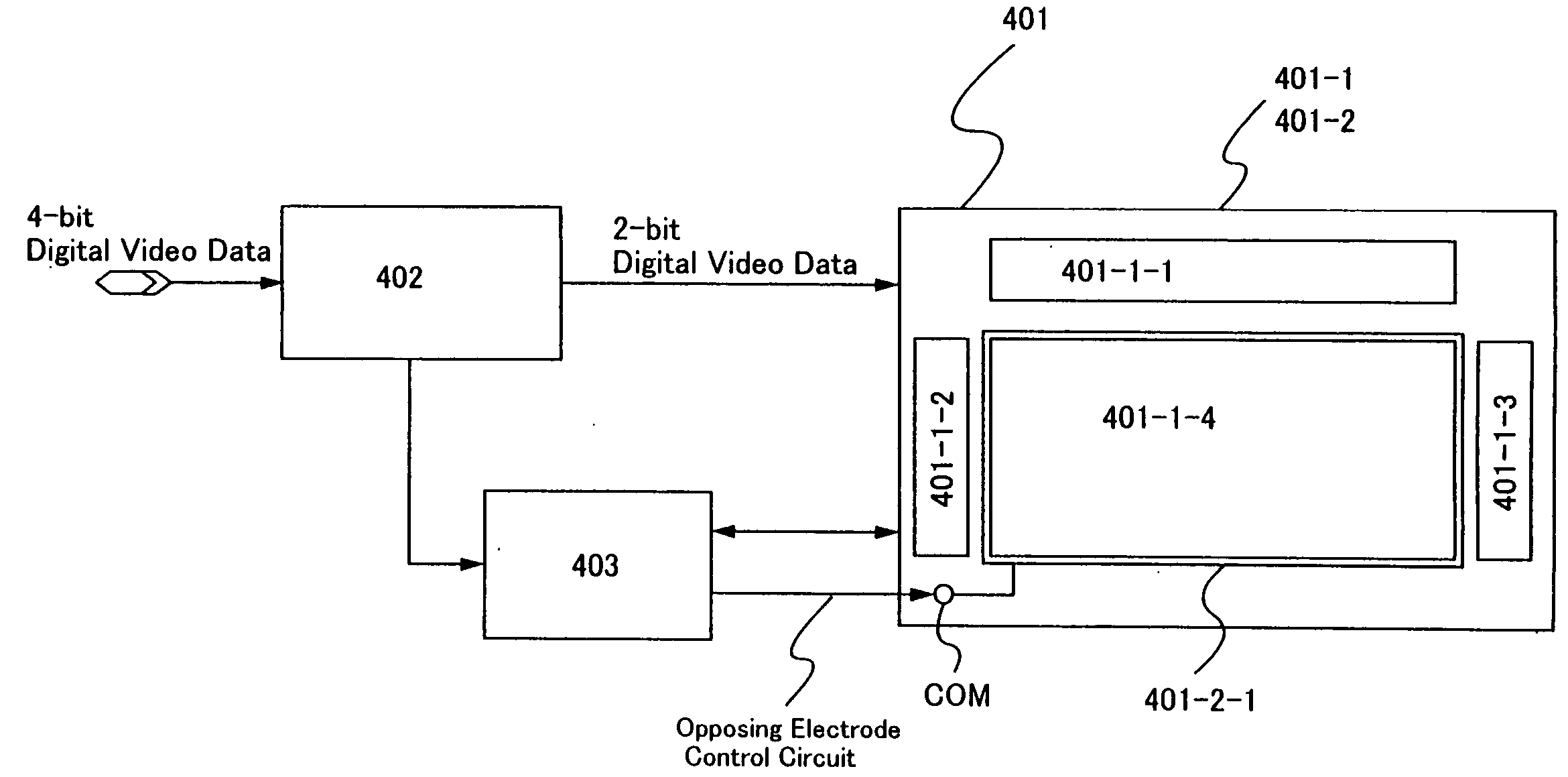
FIG. 4 schematically shows a structural diagram of a liquid crystal display device of this embodiment mode. In this embodiment mode, a liquid crystal display device to which 4 bit digital video data is sent from the external is taken as an example with the intention of simplifying the explanation.

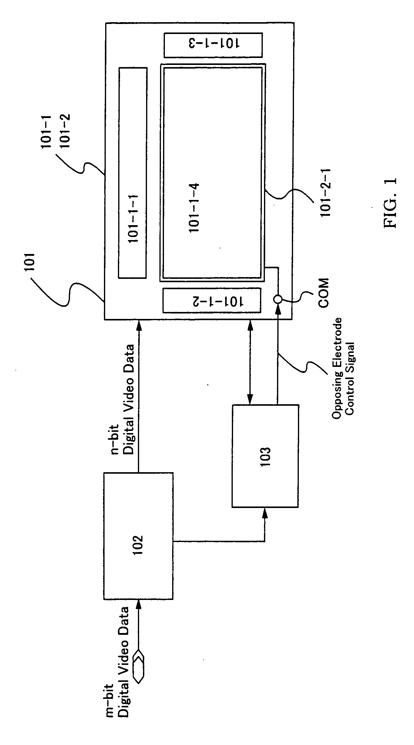
Shown in FIG. 4 is a schematic structural diagram of a liquid crystal display device according to the present invention. Reference numeral 401 denotes a liquid crystal panel having digital drivers. The liquid crystal panel 401 comprises an active matrix substrate 401-1 and an opposing substrate 401-2. The active matrix substrate 401-1 is comprised of a source driver 401-1-1, gate drivers 401-1-2 and 401-1-3, and an active matrix circuit 401-1-4 with a plurality of pixel TFTs arranged in matrix. The source driver 401-1-1 and the gate drivers 401-1-2 and 401-1-3 drive the active matrix circuit 401-1-4. The opposing substrate 401-2 has an opposing electrode 401-2-1. A terminal COM is a termi...

embodiment mode 2

This embodiment mode gives a description of a case where frame inversion driving is carried out for every sub-frame in the liquid crystal display device of the present invention which has the structure shown in Embodiment Mode 1.

Reference is made to FIG. 10. FIG. 10 shows a drive timing chart for the liquid crystal display device of this embodiment mode. The pixel P1,1, the pixel P2,1, the pixel P3,1 and the pixel Py,1 are taken as an example and shown in FIG. 10.

In this embodiment mode also, as described above, one frame term (Tf) consists of the first sub-frame term (1st Tsf), the second sub-frame term (2nd Tsf), the third sub-frame term (3rd Tsf), and the fourth sub-frame term (4th Tsf). The initialize term (Ti) is placed before every sub-frame term, and the pixel electrode initialize voltage (Vi) is applied to all the pixels during this initialize term (Ti). An opposing electrode initialize voltage (VCOMi) is also applied to the opposing electrode (COM) during the initializ...

embodiment 3

This embodiment mode employs the structure explained in Embodiment Mode 1 for the liquid crystal display device of the present invention. A description given here is about a case where only the first sub-frame term has the initialize term so that the initialize voltage (Vi and VCOM) are applied and the frame inversion driving is conducted.

Reference is made to FIG. 11. FIG. 11 shows a drive timing chart for the liquid crystal display device of this embodiment mode. The pixel P1,1, the pixel P2,1, the pixel P3,1 and the pixel Py,1 are taken as an example and shown in FIG. 11.

In this embodiment mode also, as described above, one frame term (Tf) consists of the first sub-frame term (1st Tsf), the second sub-frame term (2nd Tsf), the third subframe term (3rd Tsf), and the fourth sub-frame term (4th Tsf). The difference of this embodiment mode from Embodiment Mode 1 resides in that the initialize term (Ti) is placed before the start of the first sub-frame term only, to apply the pixe...


PUM


Abstract

An object of the present invention is to provide a small-sized active matrix type liquid crystal display device that may achieve large-sized display, high precision, high resolution and multi-gray scales. According to the present invention, gray scale display is performed by combining time ratio gray scale and voltage gray scale in a liquid crystal display device which performs display in OCB mode. In doing so, one frame is divided into subframes corresponding to the number of bit for the time ratio gray scale. Initialize voltage is applied onto the liquid crystal upon display of a subframe.

Description

BACKGROUND OF THE INVENTION 1. Field of the Invention The present invention relates to a liquid crystal display device, more specifically, a display device in which gray scale display is made by both the voltage gray scale method and the time ratio gray scale. 2. Description of the Related Art A technique that has recently accomplished rapid development is to manufacture a semiconductor device in which semiconductor thin films are formed on an inexpensive glass substrate, for example, a thin film transistor (TFT). This rapid development is caused by a growing demand for active matrix type display devices. In an active matrix display device, a pixel TFT is placed in each of pixel regions as many as several hundred thousands to several millions arranged in matrix, and electric charge that flows into and out of a pixel electrode connected to each pixel TFT is controlled by the switching function of the pixel TFT. As images are displayed with higher definition and higher resolutio...

Claims


Application Information

Patent Timeline
Patent Type & Authority Applications(United States)
IPC IPC(8): G09G3/20G09G3/36
CPCG09G3/2011G09G3/2025G09G3/2081G09G3/3614G09G3/3648G09G2320/0257G09G2300/0491G09G2310/0251G09G2310/027G09G2320/0247G09G2300/043G09G3/3607G09G3/3659G09G2300/0478H01L27/124G09G2300/0426G09G2310/0289H01L27/1222H01L27/1255H01L27/1285H01L29/78633H01L29/78675
Inventor YAMAZAKI, SHUNPEIKOYAMA, JUN
Owner SEMICON ENERGY LAB CO LTD
Why Eureka
Try Eureka