Techniques for curvature control in power transistor devices

a technology of power transistors and curvatures, applied in semiconductor devices, semiconductor/solid-state device details, electrical equipment, etc., can solve problems such as maximum heat removal

Inactive Publication Date: 2005-02-03
AGERE SYST LLC
View PDF8 Cites 42 Cited by
  • Summary
  • Abstract
  • Description
  • Claims
  • Application Information

AI Technical Summary

Problems solved by technology

However, there exists a need for power transistor processing techniques

Method used


Image

  • Techniques for curvature control in power transistor devices
  • Techniques for curvature control in power transistor devices
  • Techniques for curvature control in power transistor devices

Examples


Embodiment Construction

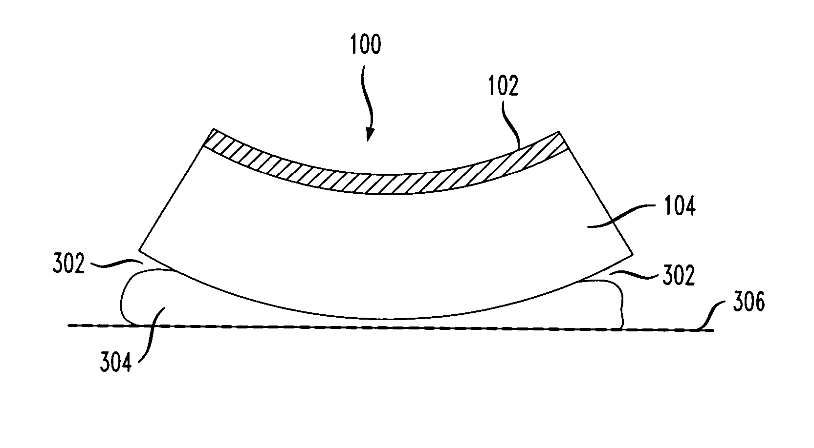
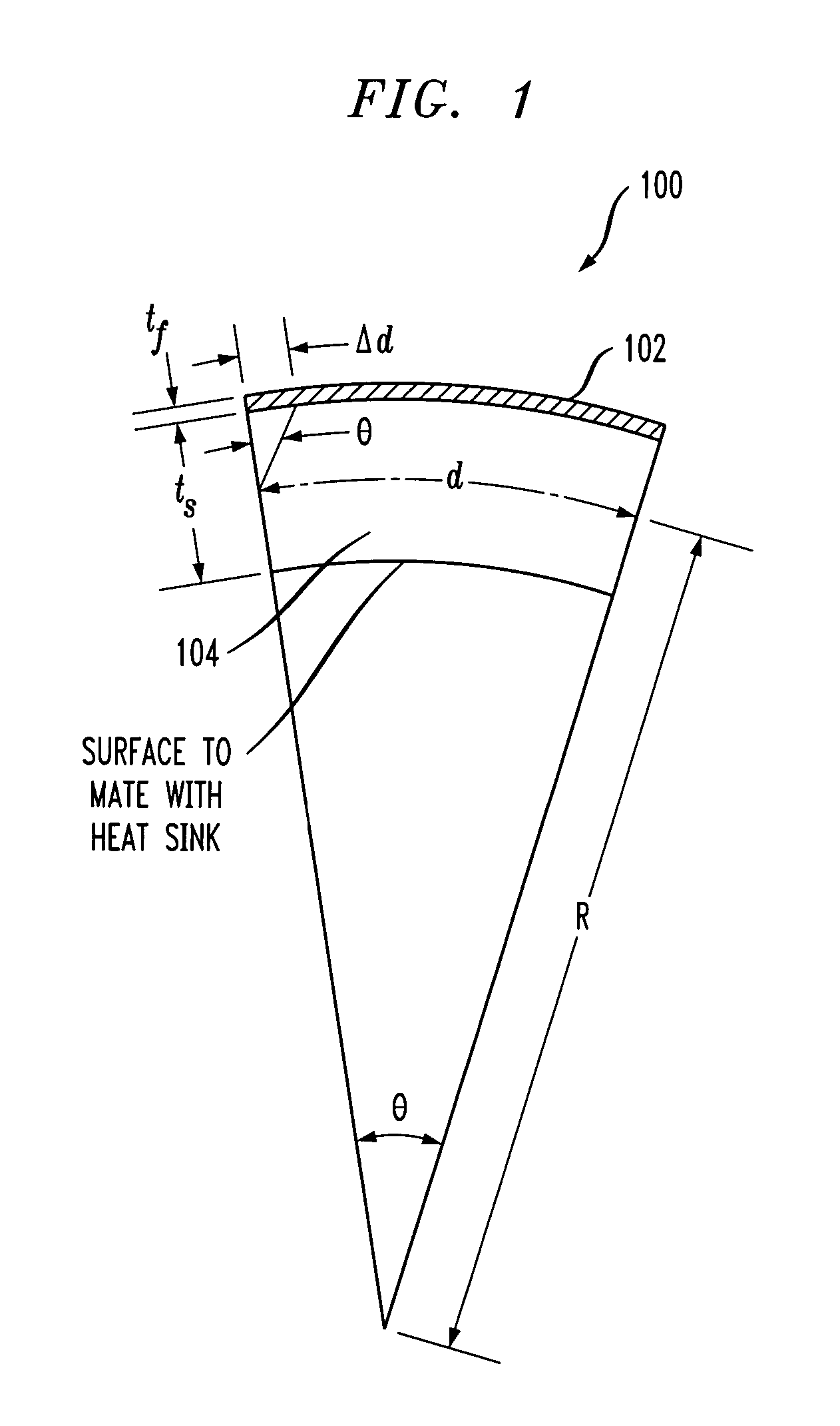
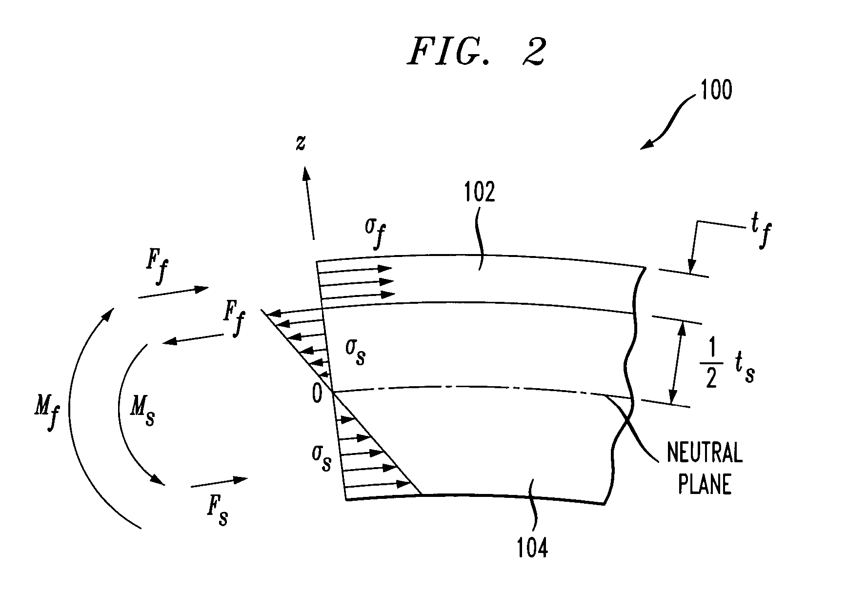
The present invention will be described below in the context of processing an exemplary power transistor device, namely a diffused metal oxide semiconductor (DMOS) device. However, it is to be understood that the present invention is not limited to use with DMOS devices. Rather, the invention is more generally applicable to the processing of any power transistor device, especially those power transistor devices requiring heat removal.

FIG. 1 illustrates an exemplary DMOS device 100 after thinning of the device substrate has been performed. DMOS device 100 comprises DMOS device film (hereinafter “DMOS film”) 102 on the surface of device substrate (hereinafter “substrate”) 104. DMOS device 100 may be, for example, part of an integrated circuit. As indicated in FIG. 1, substrate 104 may be mated with a heat sink (not shown) on a side of substrate 104 opposite DMOS film 102. DMOS film 102 represents accumulated layers that comprise DMOS device 100. For example, DMOS film 102 may includ...


PUM


Abstract

Techniques for processing power transistor devices are provided. In one aspect, the curvature of a power transistor device comprising a device film formed on a substrate is controlled by thinning the substrate, the device having an overall residual stress attributable at least in part to the thinning step, and applying a stress compensation layer to a surface of the device film, the stress compensation layer having a tensile stress sufficient to counterbalance at least a portion of the overall residual stress of the device. The resultant power transistor device may be part of an integrated circuit.

Description

FIELD OF THE INVENTION The present invention relates generally to power transistor devices, and more particularly to techniques for controlling curvature in such devices. BACKGROUND OF THE INVENTION Metal oxide semiconductor (MOS) power transistor devices have gained popularity in certain applications for their high power capabilities. There are various types of MOS power transistor devices, including diffused metal oxide semiconductor (DMOS) devices, such as Lateral DMOS (LDMOS) devices, vertical DMOS devices and trench DMOS devices. For proper operation of a power transistor device, e.g., a DMOS device, an appropriate amount of thermal coupling should exist between the current carrying channel and the metal heat sink upon which the device is mounted. Reflow mounting is a common process used to mount a power transistor device on a metal heat sink. During reflow mounting, the power transistor device is soldered to the metal heat sink. Heat removal is important for proper operati...

Claims


Application Information

Patent Timeline
IPC IPC(8): H01L21/306H01L21/331H01L21/332H01L23/31
CPCH01L21/30625H01L23/3171H01L29/66234H01L29/66363H01L2924/3011H01L2924/0002H01L2924/3511H01L2924/00
Inventor FRATTI, ROGER A.WASKIEWICZ, WARREN K.
Owner AGERE SYST LLC
Why Eureka
Try Eureka