Method of spin etching wafers with an alkali solution

a technology of spin etching and alkali solution, which is applied in the direction of basic electric elements, electrical equipment, semiconductor devices, etc., can solve the problems of acid damage to the outer edge of the top layer of the wafer, wet etching with acid poses four significant problems, and is susceptible to breakag

Inactive Publication Date: 2004-06-01
STRASBAUGH +1
View PDF29 Cites 25 Cited by
  • Summary
  • Abstract
  • Description
  • Claims
  • Application Information

AI Technical Summary

Problems solved by technology

However, stresses build up during the backgrinding process that tend to warp the wafer and make it vulnerable to breaking when the wafer is later cut into individual die.
However, wet etching with acid poses four significant problems.
First, the acid may damage the outer edge of the top layers of the wafer if the acid seeps through the protective means, such as backgrind tape, used protect the front side of the wafer.
The damage can destroy integrated chips located around the edge of the wafer, thus reducing production efficiency.
Second, using acids is inefficient.
The time required to transfer the wafers and conduct an additional process reduces the efficiency of chip production.
In addition, a machine that can perform wet etching with acid is very expensive, both initially and operationally, thus making the process more expensive and less efficient.
Third, transferring fragile wafers to a separate machine while the wafers are at a maximum state of stress increases the probability of damaging the wafers, thereby further reducing efficiency and increasing the cost of production.
Fourth, the acids typically used in the etching process are environmentally toxic and difficult to dispose of properly.
The cost of the acids, plus the cost of disposing of the acids, make the cost of using an acid wet etch process even more expensive.

Method used


Image

  • Method of spin etching wafers with an alkali solution
  • Method of spin etching wafers with an alkali solution
  • Method of spin etching wafers with an alkali solution

Examples


Embodiment Construction

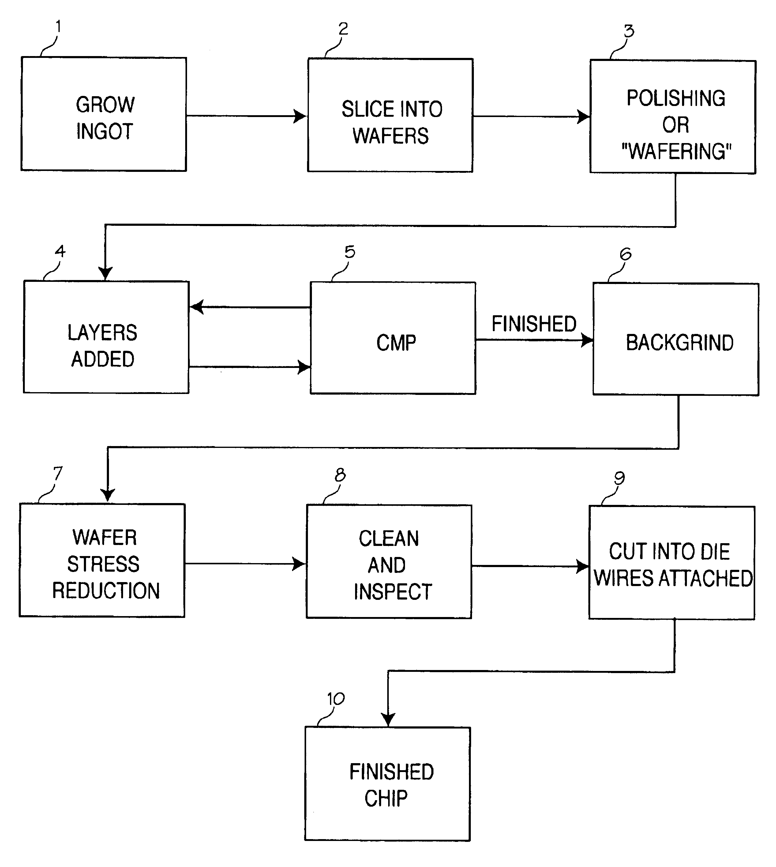
FIG. 1 is a block diagram of a system for producing integrated chips, including the backgrinding step and the step of spin etching the backside of a wafer with an alkali etch solution. In step 1 silicon is purified and cast into electronic-grade ingots. The ingots are then converted into high purity, single crystal silicon by growing a crystal silicon structure. In step 2 the ingot is sliced into wafers using a diamond saw, with each wafer being approximately 1 / 40" thick. In step 3 each wafer is polished, lapped smooth, damage decorated with acid to reveal hidden defects, and may be ground either over the wafer surface or at its edges. After the polishing processing, also known as wafering, is complete the new prime wafer is ready to have integrated circuits built upon it. In steps 4 and 5, integrated circuits are built onto the front side of the wafer. In step 4 at least one layer of material is deposited onto the silicon wafer substrate. Then, in step 5, a CMP process is applied t...


PUM


Abstract

A method of relieving surface stress on a thin wafer by removing a small portion of the wafer substrate, the substrate being removed by applying a solution of KOH to the wafer while the wafer spins.

Description

FIELD OF THE INVENTIONSThe methods and devices described below relate to the field of integrated circuit manufacture.BACKGROUND OF THE INVENTIONSTo build an integrated circuit chip, a layer of selected materials is deposited on a silicon substrate using a variety of deposition techniques, including chemical vapor deposition, sputtering, ashing, and other techniques. Chemical mechanical planarization (CMP) usually is performed after depositing the layer. CMP provides smooth, planar topographies to semiconductor wafers and surfaces deposited on a semiconductor substrate, such as silicon, and is an integral part of making many types of integrated chips. The deposition and polishing steps are repeated as necessary to build a multi-layer integrated chip. For example, a layer of electrically conducting material is sputtered onto an etched substrate. The CMP process then is used to remove the layer until the electrically conducting material remains only in the etched areas. Subsequently, a...

Claims


Application Information

Patent Timeline
Patent Type & Authority Patents(United States)
IPC IPC(8): H01L21/02H01L21/306
CPCH01L21/30608Y10S438/977
Inventor KASSIR, SALMAN M.
Owner STRASBAUGH
Why Eureka
Try Eureka