Flat panel display and method of fabricating the same

Active Publication Date: 2005-02-10
SAMSUNG DISPLAY CO LTD
View PDF2 Cites 26 Cited by
  • Summary
  • Abstract
  • Description
  • Claims
  • Application Information

AI Technical Summary

Benefits of technology

[0019] The present invention provides a top-emitting organic light-emitting display device (OLED) and

Problems solved by technology

A conventional organic light-emitting OLED device having a structure as described above typically uses a poly-silicon film TFT, and suffers decreased contrast when the EL element emits light.
In the case of mobile displays in particular, which are extensively exposed to exterior light, this is a serious problem because the contrast is drastically decreased by the internal reflections of the exterior light.
In order to prevent reduction of contrast due to the reflection of exterior light, an expensive polarizer is typically attached to a front surface of the display device.
This leads to other problems in that addition of the expensive polarizer

Method used


Image

  • Flat panel display and method of fabricating the same
  • Flat panel display and method of fabricating the same
  • Flat panel display and method of fabricating the same

Examples


Embodiment Construction

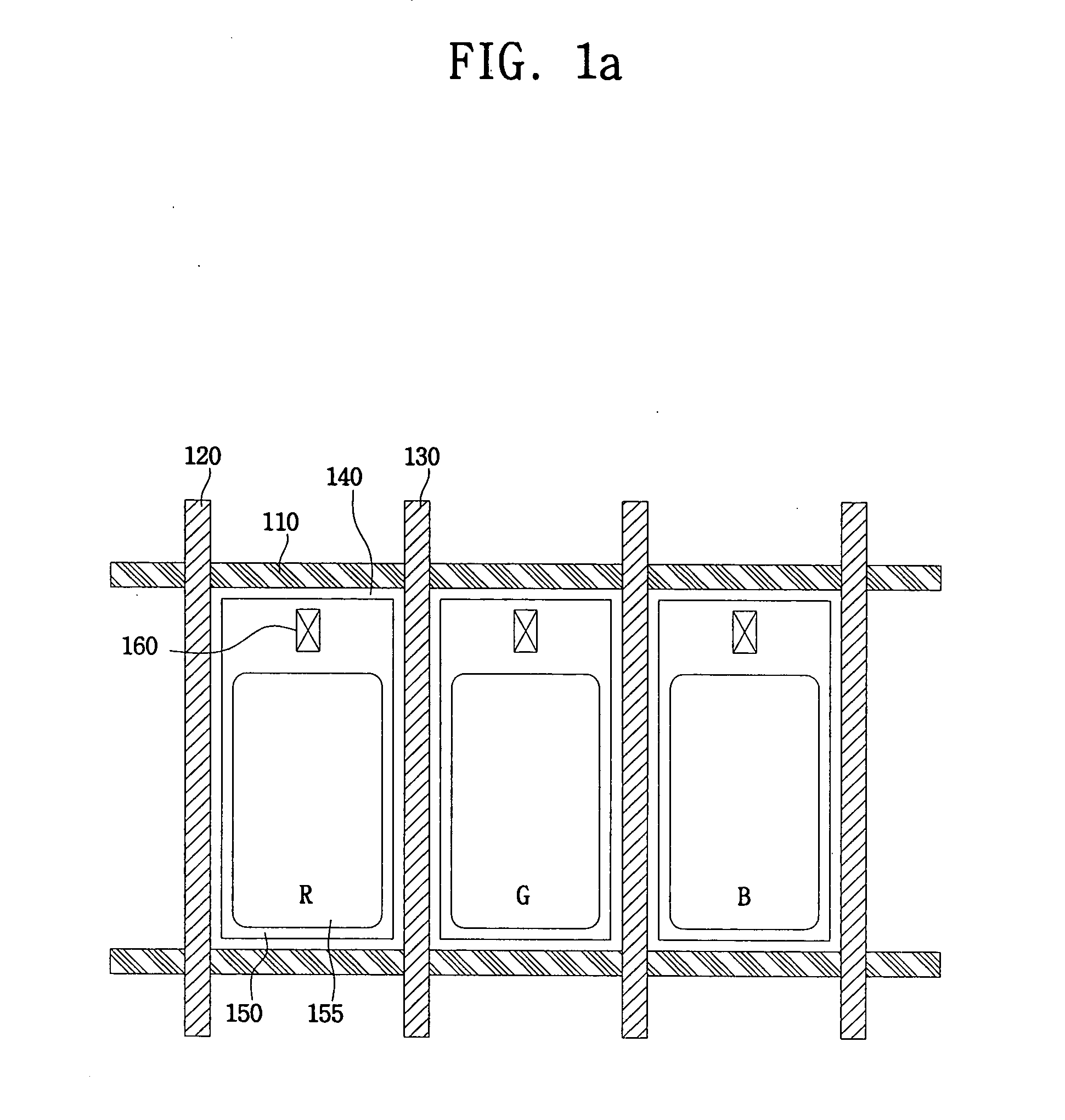
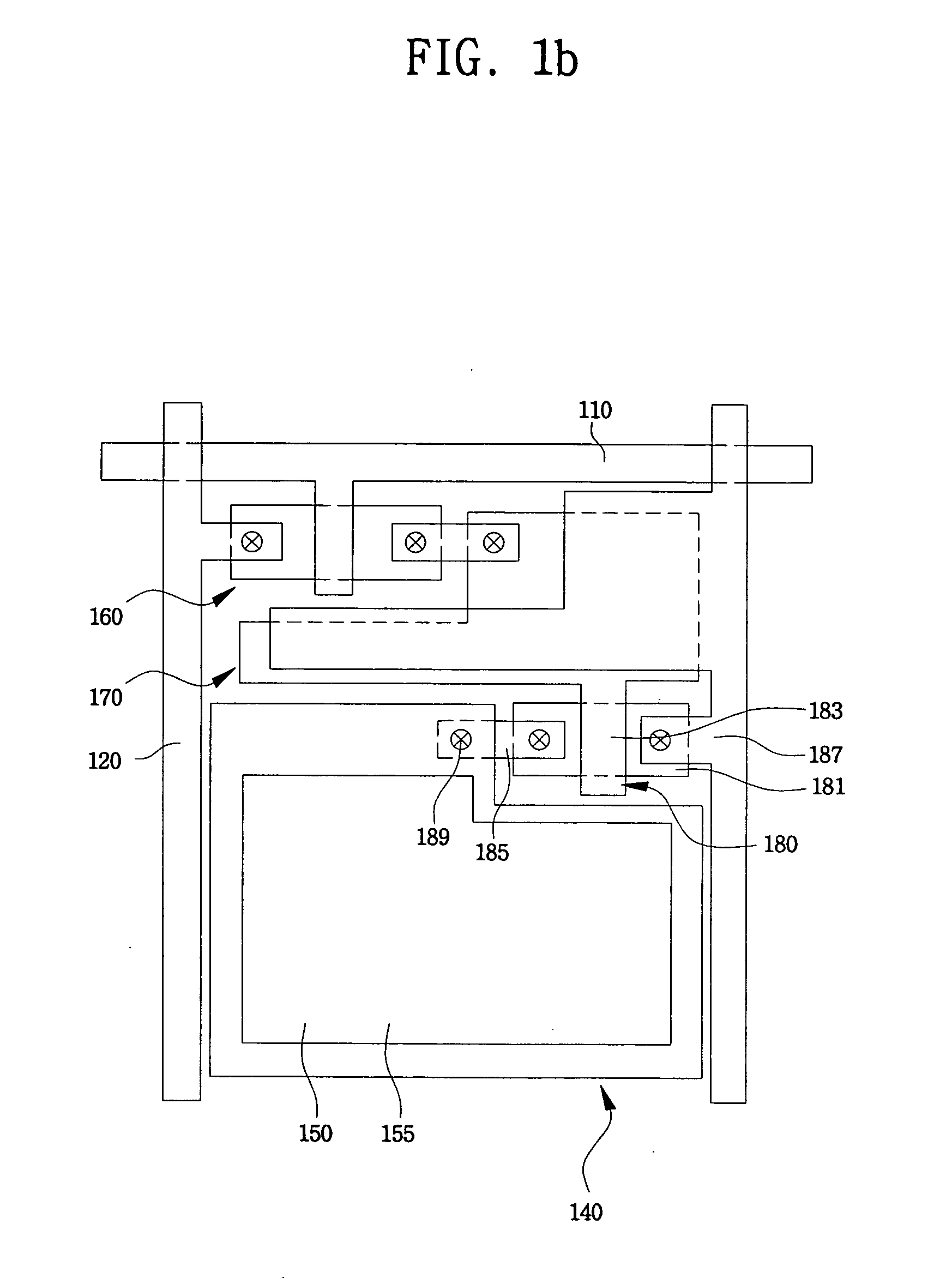
[0031]FIG. 3 is a top view of a portion 300 of an ALOMED organic light-emitting device, configured in accordance with an embodiment of the present invention, illustrating a configuration of red (R), green (G) and blue (B) unit pixels.

[0032] As FIG. 3 illustrates, a plurality of gate lines 310, insulated from each other, are arranged in one direction; a plurality of data lines 320; insulated from each other, are arranged in a direction crossing the gate lines 310; a plurality of power lines 330, also insulated from each other, cross the gate lines 310, and are arranged in parallel with the data lines 320, a plurality of pixel portions 340 are formed within an area bounded by the gate lines 310, the data lines 320, and the power lines 330; and a plurality of pixel electrodes 350 are arranged in each of the pixel portions 340 and have openings 355. In order not to unnecessarily complicate FIG. 3A, reference numerals applicable to each of the R, G, B unit pixels are indicated on only t...


PUM


Abstract

A light-emitting display device the same includes an insulating substrate having a thin film transistor formed thereon. The thin film transistor includes a source electrode and/or a drain electrode. A passivation layer is formed on the insulating substrate over at least a portion of the thin film transistor, and has a via hole formed therein, which electrically contacts either the source electrode or the drain electrode. A pixel electrode is formed in the via hole. A light-blocking layer is formed over an entire upper surface of the passivation layer except for an area corresponding to the pixel electrode. A planarization layer is formed on an upper surface of the light-blocking layer except for an area corresponding to the pixel electrode.

Description

CROSS-REFERENCE TO RELATED APPLICATION [0001] This application claims priority of Korean Patent Application No. 10-2003-0054795, filed Aug. 7, 2003, which is hereby incorporated by reference. BACKGROUND OF THE INVENTION [0002] 1. Field of the Invention [0003] The present invention relates to flat panel displays generally, and more particularly, to an organic light-emitting display (OLED) device and method of fabricating the same, which improves contrast by independently forming a light-blocking layer on an entire surface between a thin film transistor (TFT) and an electrode (EL) element. [0004] 2. Description of the Related Art [0005]FIG. 1A is a top view of a portion 100 conventional active-matrix organic light emitting display device (AMOLED), illustrating red (R), green (G) and blue (B) unit pixels. FIG. 1B is a top view of a unit pixel 140 used in a portion 100 of the conventional AMOLED shown in FIG. 1A. [0006] In order not to unnecessarily complicate FIG. 1A., reference numera...

Claims


Application Information

Patent Timeline
IPC IPC(8): H01L27/32H01L51/50H05B33/02H01L51/52H05B33/00H05B33/10H05B33/12H05B33/14H05B33/22H05B44/00
CPCH01L27/3244H01L2251/5346H01L51/5284H10K59/12H10K50/865H10K2101/80H05B33/22
Inventor PARK, SANG-IIKOO, JAE-BONLEE, HUN-JUNG
Owner SAMSUNG DISPLAY CO LTD
Why Eureka
Try Eureka