Method for processing a semiconductor wafer

a technology of semiconductor wafers and processing methods, applied in semiconductor/solid-state device manufacturing, basic electric elements, electric devices, etc., can solve the problems that the future semiconductor manufacturing process may ultimately require more control and economic efficiency from the reactor, and achieve the effect of convenient removal and service, and convenient re-configuration

Inactive Publication Date: 2005-02-10
SEMITOOL INC
View PDF99 Cites 4 Cited by
  • Summary
  • Abstract
  • Description
  • Claims
  • Application Information

AI Technical Summary

Benefits of technology

[0010] Additionally, the reactor includes several advantageous mechanical features including those that allow the reactor to be used with robotic wafer transfer equipment, those that allow the reactor to be readily re-configured for different processes, and those that allow the processing chamber of the reactor to be easily removed and serviced.

Problems solved by technology

However, it has now been recognized that demands for future semiconductor manufacturing processes may ultimately require more control and economic efficiency from the reactor.

Method used


Image

  • Method for processing a semiconductor wafer
  • Method for processing a semiconductor wafer
  • Method for processing a semiconductor wafer

Examples


Embodiment Construction

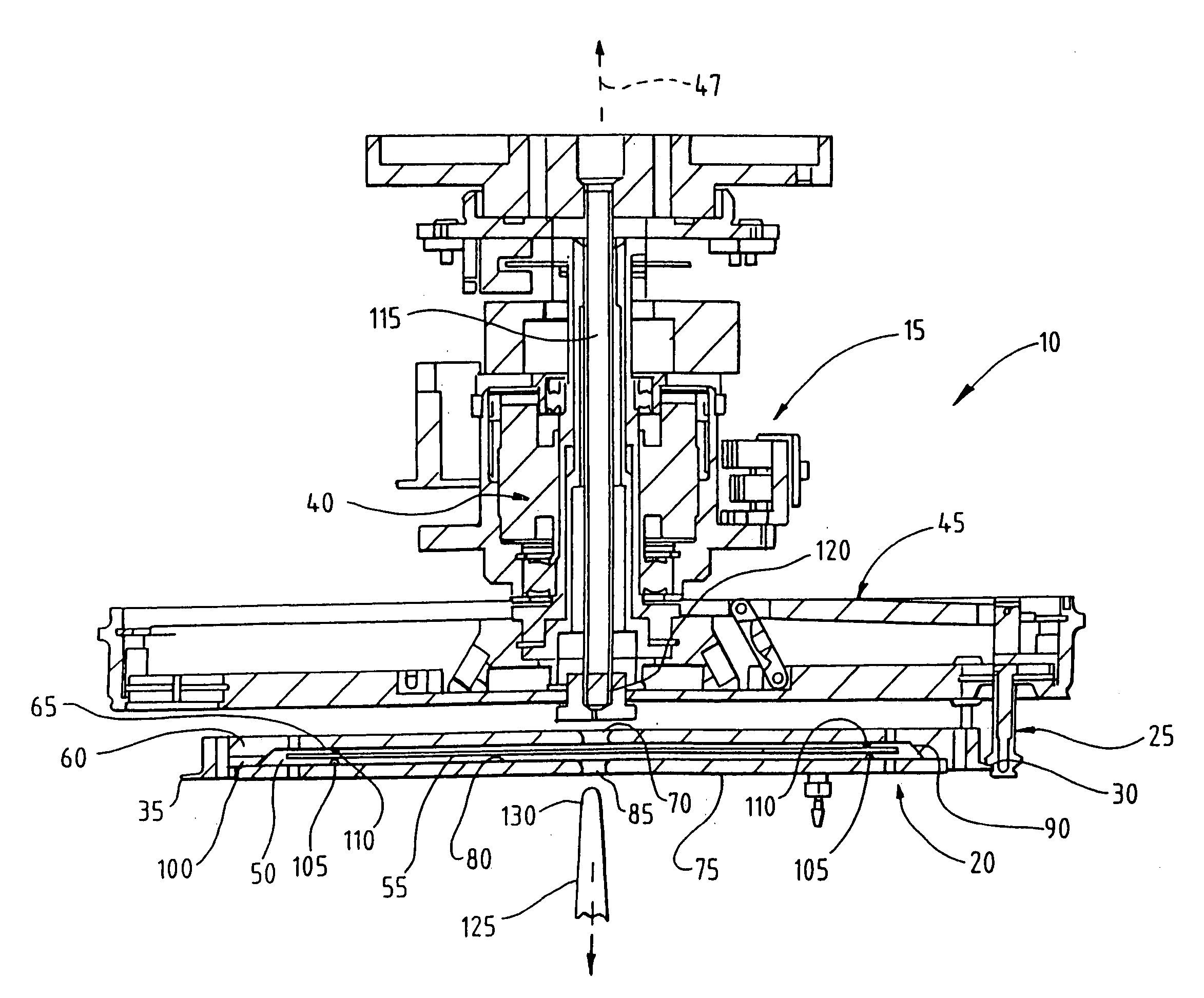
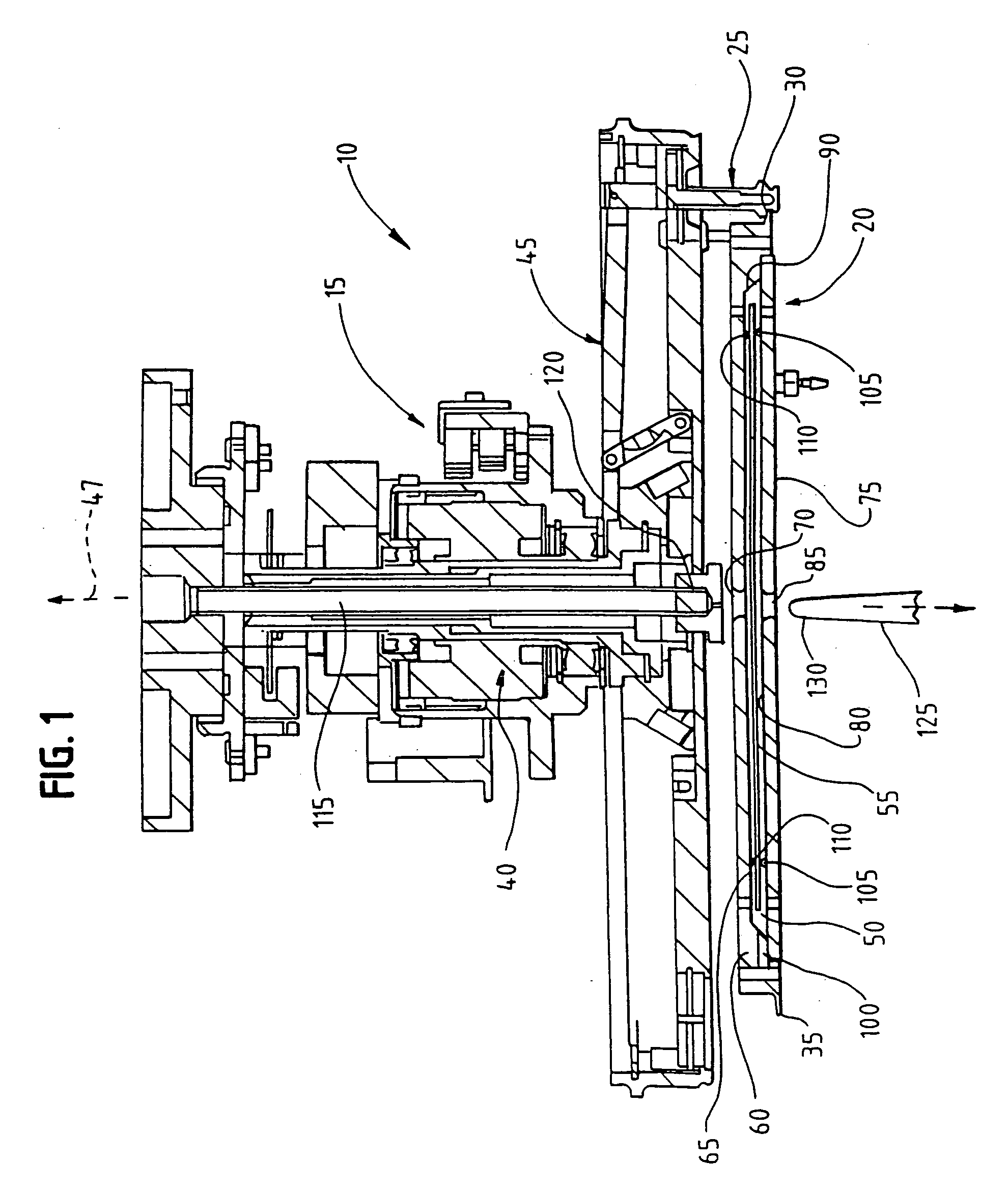
[0037]FIG. 1 is a cross-sectional view of one embodiment of a reactor, shown generally at 10, constructed in accordance with the teachings of the present invention. The embodiment of the reactor 10 of FIG. 1 is generally comprised of a rotor portion 15 and a microelectronic workpiece housing 20. The rotor portion 15 includes a plurality of support members 25 that extend downwardly from the rotor portion 15 to engage the workpiece housing 20. Each of the support members 25 includes a groove 30 that is dimensioned to engage a radially extending flange 35 that extends about a peripheral region of the workpiece housing 20. Rotor portion 15 further includes a rotor motor assembly 40 that is disposed to rotate a hub portion 45, including the support members 25, about a central axis 47. Workpiece housing 20 is thus secured for co-rotation with hub portion 45 when support members 25 are engaged with flange 35. Other constructions of the rotor portion 15 and the engagement mechanism used for...


PUM

PropertyMeasurementUnit
thicknessaaaaaaaaaa
distanceaaaaaaaaaa
widthaaaaaaaaaa

Abstract

An apparatus for processing a semiconductor wafer or similar article includes a reactor having a processing chamber formed by upper and lower rotors. The wafer is supported between the rotors. The rotors are rotated by a spin motor. A processing fluid is introduced onto the top or bottom surface of the wafer, or onto both surfaces, at a central location. The fluid flows outwardly uniformly and in all directions. A wafer support automatically lifts the wafer, so that it can be removed from the reactor by a robot, when the rotors separate from each other after processing.

Description

[0001] This Application is a Continuation of U.S. patent application Ser. No. 10 / 202,074, filed Jul. 23, 2002, and now pending, and incorporated herein by reference, which is a is a Continuation of U.S. patent application Ser. No. 09 / 437,711, filed Nov. 10, 1999, now U.S. Pat. No. 6,423,642, which is: [0002] 1) a Continuation-In-Part of and U.S. National Phase of International Patent Application No. PCT / US99 / 05676, filed Mar. 15, 1999; [0003] 2) a Continuation-In-Part of U.S. patent application Ser. No. 09 / 113,435, filed Jul. 10, 1998, now U.S. Pat. No. 6,264,752; [0004] 3) a Continuation-in-Part of U.S. patent application Ser. No. 09 / 041,901, filed Mar. 13, 1998, now U.S. Pat. Nos. 6,350,319; and [0005] 4) a Continuation-in-Part of U.S. patent application Ser. No. 60 / 116,750 filed Jan. 23, 1999.BACKGROUND OF THE INVENTION [0006] The semiconductor manufacturing industry is constantly seeking to improve the processes used to manufacture microelectronic circuits and components, such a...

Claims


Application Information

Patent Timeline
Patent Type & Authority Applications(United States)
IPC IPC(8): H01L21/306B08B3/04H01L21/00H01L21/3213
CPCB08B3/04H01L21/32134H01L21/67017H01L21/67051Y10S118/90H01L21/6715Y10S438/906Y10S438/913H01L21/6708
Inventor PEACE, STEVEN L.CURTIS, GARY L.THOMPSON, RAYMON F.AEGERTER, BRIANDUNDAS, CURT T.
Owner SEMITOOL INC
Why Eureka
Try Eureka