Multiplexer with low parasitic capacitance effects

a capacitance effect and multi-channel amplifier technology, applied in the field of multi-channel amplifiers, can solve the problems of inter-symbol interference, isi, and performance degradation of cascaded arrays of amplifiers at high clock and input signal frequencies, and achieve the effect of reducing inter-symbol interferen

Inactive Publication Date: 2005-02-17
AVAGO TECH INT SALES PTE LTD
View PDF18 Cites 11 Cited by
  • Summary
  • Abstract
  • Description
  • Claims
  • Application Information

AI Technical Summary

Benefits of technology

[0031]FIG. 8 illustrates a reduction in inter-symbol interference using the present invention.

Problems solved by technology

Unfortunately, the performance of cascaded arrays of amplifiers degrades significantly at high clock and input signal frequencies.
This translates into non-linearity of the ADC, and often causes inter-symbol interference (ISI).
The problem of ISI occurs in most, if not all, ADC architectures and various approaches exist for attacking the problem.
However, the resulting increase in power consumption is a major disadvantage.
However, this increases required layout area.
Furthermore, mismatches between the interleaved channels cause spurious tones.
Unfortunately, this is not optimal for high speed operation either.
This effect is undesirable in multiplexers.
However, this approach has two problems.

Method used


Image

  • Multiplexer with low parasitic capacitance effects
  • Multiplexer with low parasitic capacitance effects
  • Multiplexer with low parasitic capacitance effects

Examples


Embodiment Construction

[0036] Reference will now be made in detail to the preferred embodiments of the present invention, examples of which are illustrated in the accompanying drawings.

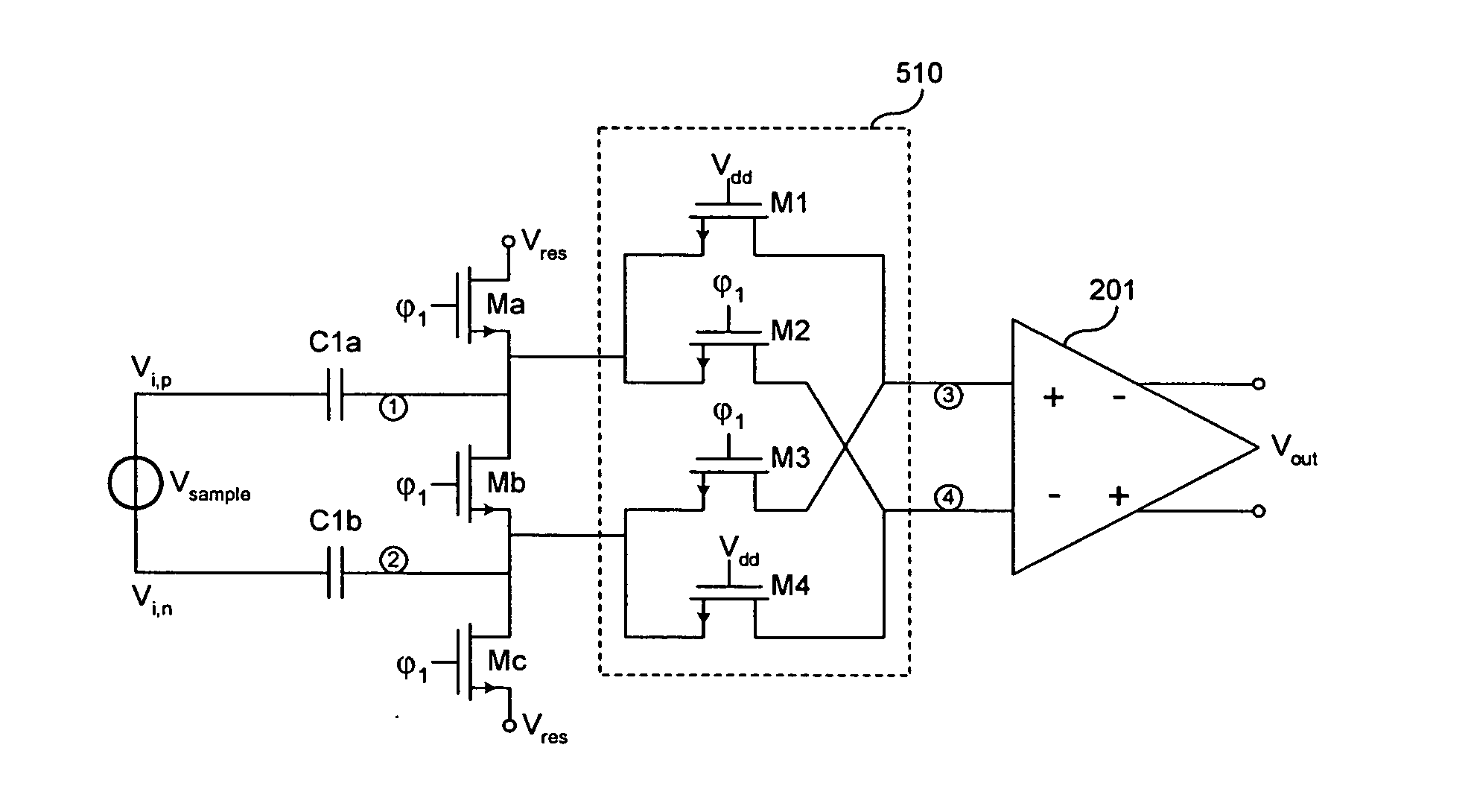
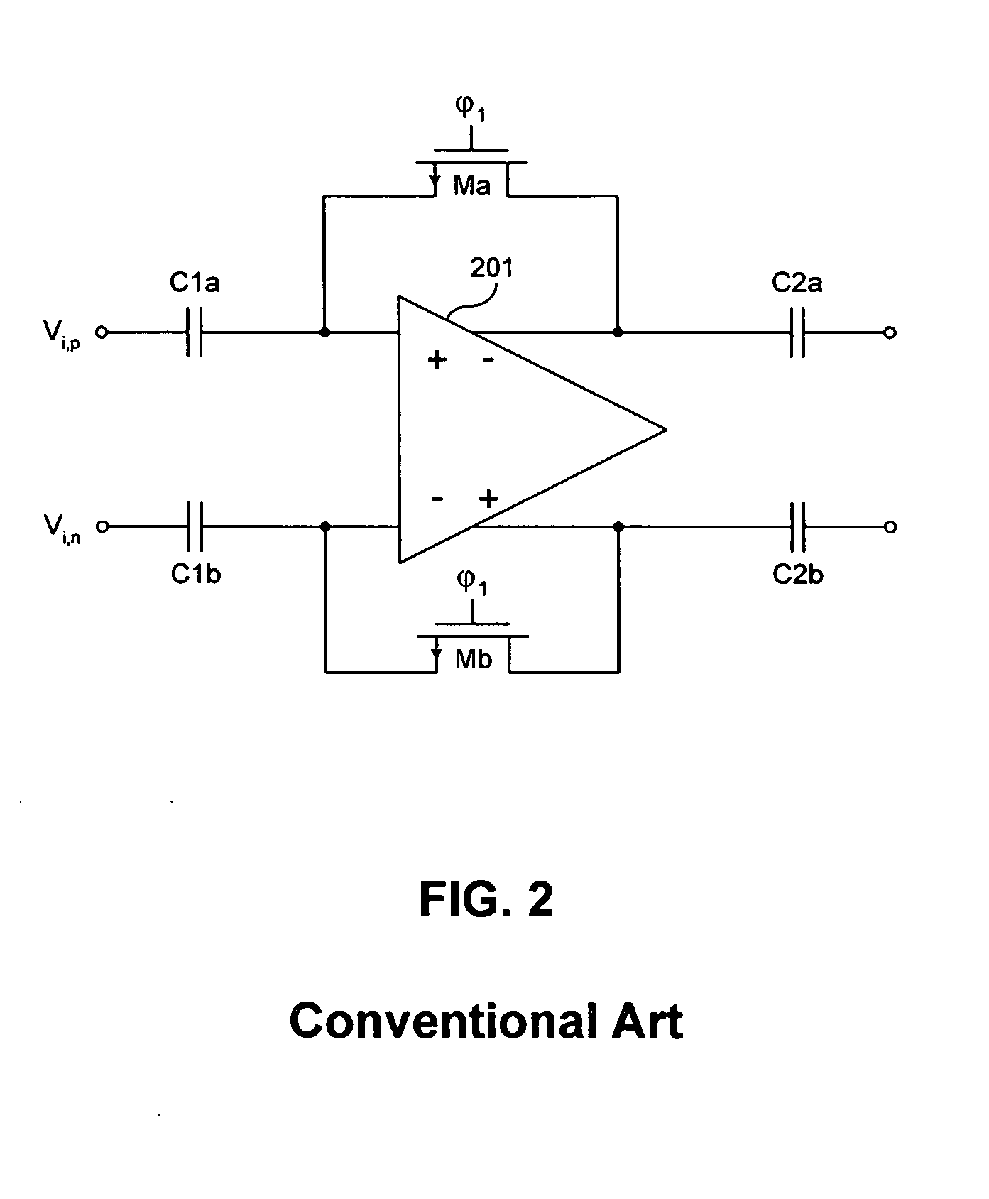
[0037] Recently, a technique to address the nonlinearity was published by Miyazaki et al., “A 16 mW 30 M Sample / s pipelined A / D converter using a pseudo- differential architecture,” ISSCC Digest of Tech. Papers, pp. 174-175 (2002), see particularly FIG. 10.5.2 therein. The technique applies only to amplifiers that use the auto-zero technique of FIG. 2.

[0038] In Miyazaki, four extra switches and two extra capacitors are required. The resulting circuit topology has a common-mode transfer function of “1” and a differential-mode transfer function of “0” during the reset clock phase.

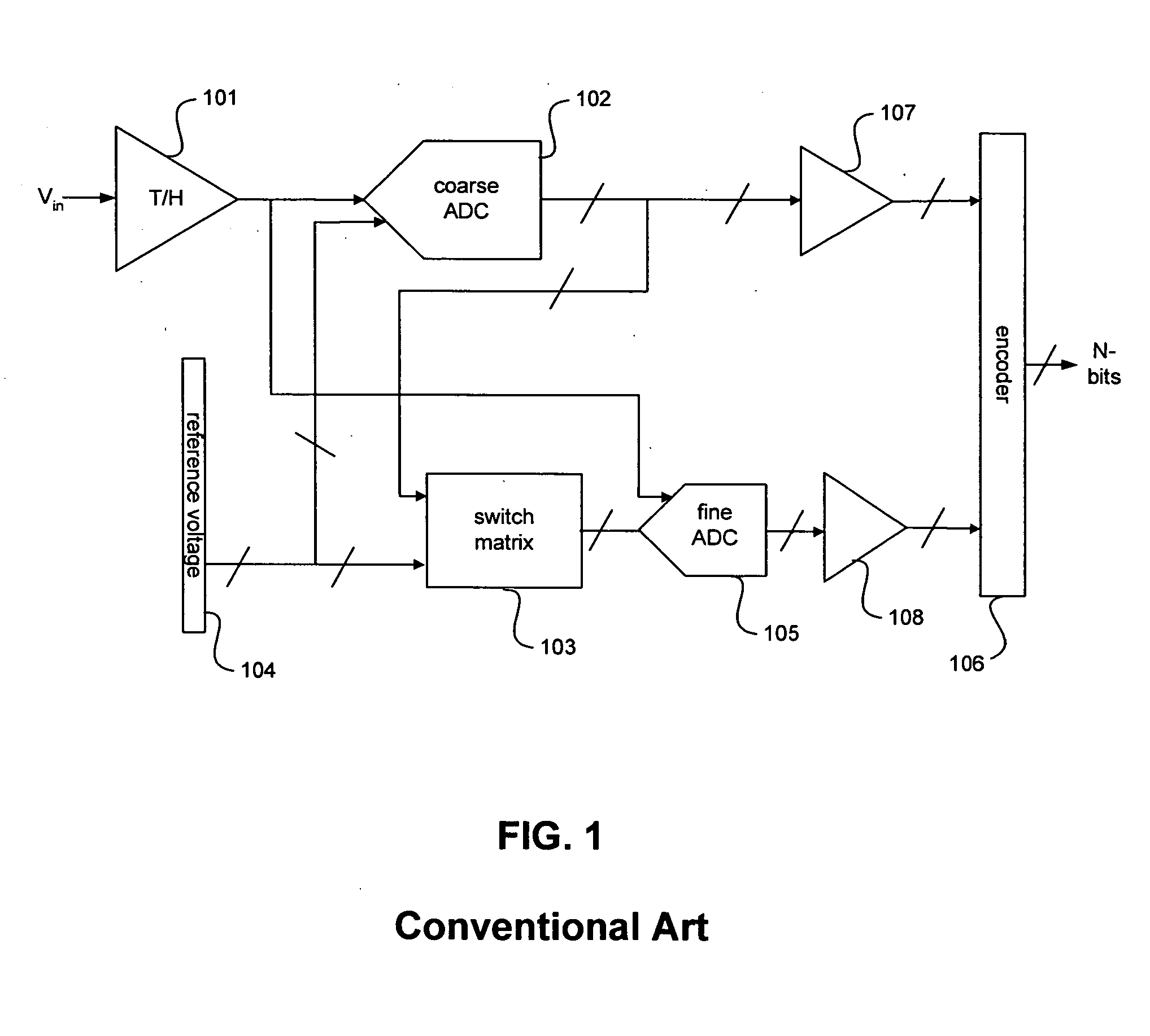
[0039] However, an important disadvantage of the circuit shown in Miyazaki is that it requires twice the amount of capacitance. This has a serious impact on the ADC layout area. Furthermore, the capacitive loading of the track-and-hold 101 doubles...


PUM


Abstract

A differential multiplexer includes a plurality of multiplexing circuits. Each multiplexing circuit inputs a corresponding differential input signal including a positive input signal and a negative input signal, and outputs positive and negative output signals. Each multiplexing circuit includes first, second, third and fourth transistors. The first and second transistors input the positive input signal. The third and fourth transistors input the negative input signal. Outputs of the first and third transistors are connected to the positive output signal. Outputs of the second and fourth transistors are connected to the negative output signal. The positive and negative output signals are controlled using gate voltages on the first and fourth transistors. The second and third transistors are turned off when the differential multiplexer is in use. The transistors are cross-coupled to make leakage between the positive and negative input signals common mode in the positive and negative output signals.

Description

CROSS-REFERENCE TO RELATED APPLICATIONS [0001] This application is a Continuation-in-part of application Ser. No. 10 / 893,999, Filed: Jul. 20, 2004, Titled: HIGH SPEED ANALOG TO DIGITAL CONVERTER, which is a Continuation of application Ser. No. 10 / 688,921, Filed: Oct. 21, 2003, Titled: HIGH SPEED ANALOG TO DIGITAL CONVERTER, which is a Continuation of application Ser. No. 10 / 349,073, Filed: Jan. 23, 2003, Titled: HIGH SPEED ANALOG TO DIGITAL CONVERTER, which is a Continuation of application Ser. No. 10 / 158,595, Filed: May 31, 2002, Titled: HIGH SPEED ANALOG TO DIGITAL CONVERTER, all of which are incorporated by reference herein.BACKGROUND OF THE INVENTION [0002] 1. Field of the Invention [0003] The present invention relates to multiplexers, and, more particularly, to multiplexers with low cross-talk between signals. [0004] 2. Related Art [0005] A subranging analog to digital converter (ADC) architecture is suitable for implementing high-performance ADC's (i.e. high speed, low power, ...

Claims


Application Information

Patent Timeline
Patent Type & Authority Applications(United States)
IPC IPC(8): H03M1/36
CPCH03K17/002H03M1/365H03M1/36H03K17/145
Inventor MULDER, JANVAN DER GOES, FRANCISCUS MARIA LEONARDUS
Owner AVAGO TECH INT SALES PTE LTD
Why Eureka
Try Eureka