Pulse Harmonic Modulation Systems And Methods

a harmonic modulation and pulse technology, applied in the field of pulse harmonic modulation systems and methods, can solve the problems of increased power loss, impracticality of high carrier frequencies for imds, high data transmission bandwidth, etc., and achieve the effect of reducing inter-symbol interferen

Inactive Publication Date: 2012-11-22
GEORGIA TECH RES CORP
View PDF3 Cites 13 Cited by
  • Summary
  • Abstract
  • Description
  • Claims
  • Application Information

AI Technical Summary

Benefits of technology

[0019]The present invention relates to pulse harmonic modulation systems and methods. An exemplary embodiment of the present invention provides a pulse harmonic modulation method. The method comprises transmitting a first data initiation pulse to an input of a first resonant circuit thereby creating an oscillating waveform at an output of a second resonant circuit. The method further comprises transmitting a first modifying pulse to the input of the first resonant circuit, wherein the first modifying pulse reduces the inter-symbol interference at the output of the second resonant circuit by modifying a first portion of the oscillating waveform at the output of the second resonant circuit.
[0022]In addition to pulse harmonic modulation methods, the present invention relates to pulse harmonic modulation systems. An exemplary embodiment of the present invention provides a pulse harmonic modulation system. The pulse harmonic modulation system can comprise a first resonant circuit in communication with a second resonant circuit, wherein the first resonant circuit is enabled to receive a first data initiation pulse, which causes an oscillating waveform at an output of the second resonant circuit, and the first resonant circuit is enabled to receive a first modifying pulse to reduce inter-symbol interference at the output of the second resonant circuit by modifying a first portion of the oscillating waveform.

Problems solved by technology

Achieving high power transmission efficiency, high data transmission bandwidth, and small size while maintaining robustness and a low Bit-Error-Rate (“BER”) against impediments, such as external interference, supply ripple, load changes, internal digital switching noise, and coupling variations due to vibrations and coils misalignments, are some of the major challenges in the design of conventional inductive coupling systems.
However, it is clear that a high data transmission bandwidth is needed for wireless implantable microstimulators that interface with the CNS.
Such high carrier frequencies, however, are impractical for use in IMDs.
The maximum carrier frequency for biomedical implants is limited to a few tens of MHz (generally 20˜30 MHz) due to the coupled coils' self-resonance frequency, increased power loss in the power transmission circuitry at higher carrier frequencies, and excessive power dissipation in the tissue, which increases as the carrier frequency squared (fr2).
ASK, however, is not robust against coupling variations and faces major limitations for high-bandwidth data transmission.
This requires large capacitors that cannot be easily integrated in the low-frequency end of RF applications.
Even with OOK, however, achieving high data-rates is challenging, and data rates are usually less than 10% of the carrier frequency.
A limitation with FSK is that it occupies a relatively wide bandwidth (>5 MHz).
However, the dependence of all of these methods on a carrier signal results in high power consumption, particularly on the transmitter side of the transmissions system.
As a result, the RF transmitter is one of the key power consuming blocks in such IMDs.
LSK is limited because of its requirement for strong coupling between coils, a switch across the IMD power coil, and an ASK receiver outside of the body.
Although the switch is relatively simple to implement and consumes little power, the switch entirely shuts off the power transfer to the IMD when it is closed.
Hence, a fundamental problem with LSK is reducing the IMD received power by the switching duty cycle, which is not desired in high performance IMDs.
There are, however, problems with using these UWB methods in applications where a power carrier is present.
The power carrier interference can dominate the data carrier on the receiver side, such that data recovery becomes nearly impossible.
This results in ringing on the Rx side that extends well beyond the designated bit period.
This will either increase the ISI and BER or lead to data rate reduction—both of which are undesirable.
Maintaining high SRF in 100's of MHz range in implanted coils, which are used in IMDs, is not quite feasible because the coils' dimensions, inductance, an separation are often much larger and their parasitic resistance is much lower than that of the on-chip coils used in chip-to-chip communication.
Therefore, many of these conventional methods are inapplicable in IMDs.
Unlike coils used in IMDs, on-chip coils inevitably have low Qs due to their high parasitic resistance.
Low Q, however, has the undesirable effect of decreasing the range of the inductive link, i.e. the maximum coil separation.
This occurs because the amplitude of the received signal decreases and the noise and interference due to lowering the receiver selectivity increases, which, consequently, degrades the Rx Signal-to-Noise Ratio (“SNR”).

Method used


Image

  • Pulse Harmonic Modulation Systems And Methods
  • Pulse Harmonic Modulation Systems And Methods
  • Pulse Harmonic Modulation Systems And Methods

Examples


Embodiment Construction

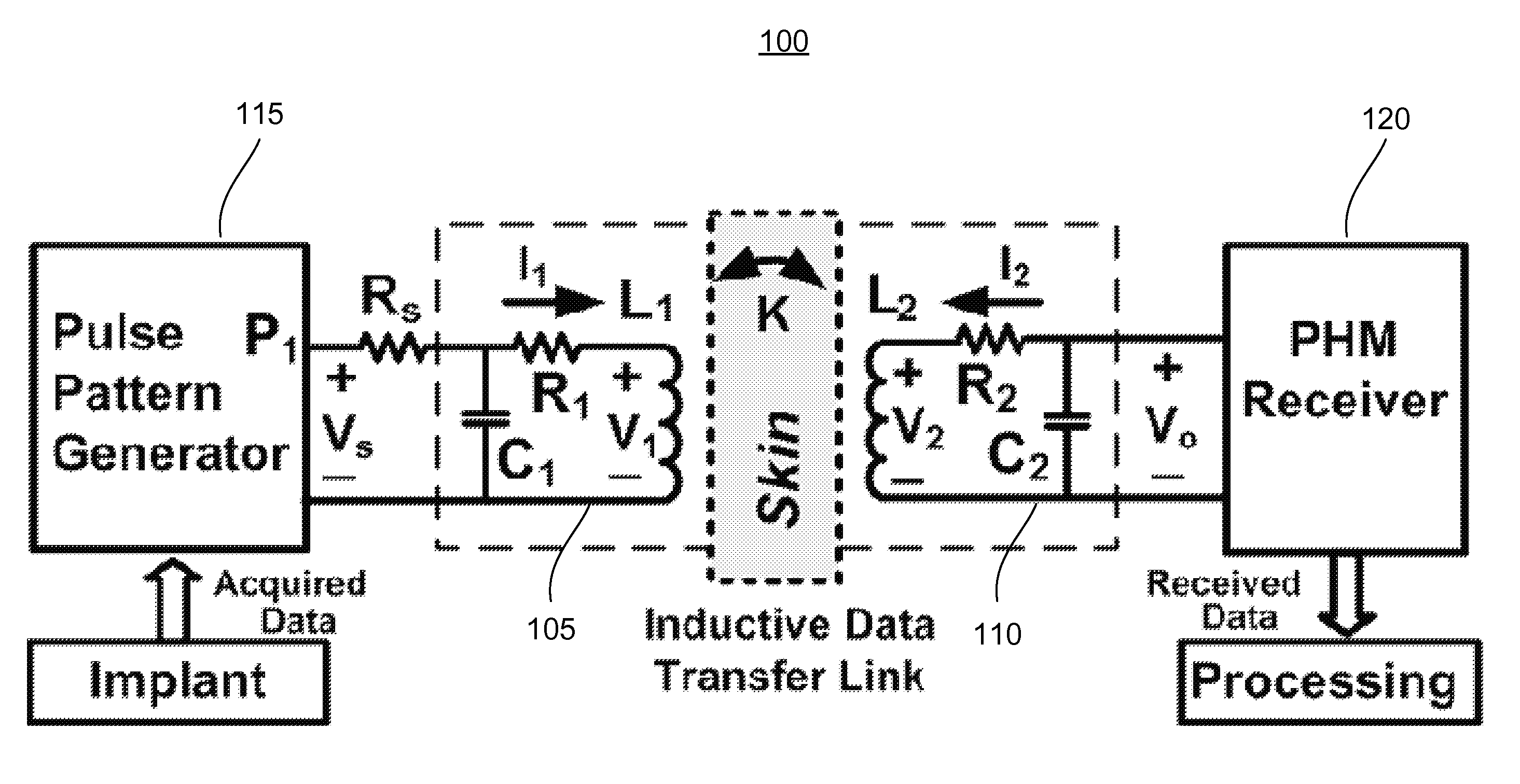
[0046]To facilitate an understanding of the principles and features of the present invention, various illustrative embodiments are explained below. In particular, the invention is described in the context of being pulse harmonic modulation systems and methods. Embodiments of the present invention may be applied to systems or methods for transmitting data via an inductive link. Embodiments of the invention, however, are not limited to use in systems and methods for transmitting data via an inductive link described herein. As those of ordinary skill in the art would understand, embodiments of the invention can be used by any systems or methods for transmitting data via an inductive link, including, but not limited to, IMD systems, RFID systems, contactless smartcards, MEMS, and the like. Additionally, embodiments of the present invention can be used to transmit data in both near-field and far-field applications.

[0047]The components described hereinafter as making up various elements o...


PUM


Abstract

The various embodiments of the present disclosure relate generally to pulse harmonic modulation systems and methods. An embodiment of the present invention provides a pulse harmonic modulation method comprising transmitting a first data initiation pulse to an input of a first resonant circuit thereby creating an oscillating waveform at an output of a second resonant circuit and transmitting a first modifying pulse to the input of the first resonant circuit. The first modifying pulse can modify a first portion of the oscillating waveform.

Description

CROSS-REFERENCE TO RELATED APPLICATIONS[0001]This application claims the benefit of U.S. Provisional Application Ser. No. 61 / 267,965, filed 9 Dec. 2009, and U.S. Provisional Application Ser. No. 61 / 378,629, filed 31 Aug. 2010, both of which are incorporated herein by reference in their entireties as if fully set forth below.STATEMENT REGARDING FEDERALLY SPONSORED RESEARCH[0002]This invention was made with U.S. Government support under Grant No. ECCS-0824199 awarded by the National Science Foundation. The U.S. Government has certain rights in the invention.TECHNICAL FIELD OF THE INVENTION[0003]The various embodiments of the present disclosure relate generally to modulation systems and methods. More particularly, the various embodiments of the present invention are directed to pulse harmonic modulation systems and methods.BACKGROUND OF THE INVENTION[0004]Near-field inductive links have been extensively used in conventional methods for short-range data and power transmission. An induct...

Claims


Application Information

Patent Timeline
Patent Type & Authority Applications(United States)
IPC IPC(8): H04L27/00H04B5/00
CPCA61N1/3727A61N1/37223
Inventor GHOVANLOO, MAYSAMINANLOU, FARZAD
Owner GEORGIA TECH RES CORP
Why Eureka
Try Eureka