Integrated circuit stacking system and method

a stacking system and integrated circuit technology, applied in the direction of printed circuit aspects, printed circuit non-printed electric components association, electrical apparatus construction details, etc., can solve the problems of large expense, lack of stacking chip scale package technology, and high cost and complexity

Inactive Publication Date: 2005-02-24
ENTORIAN TECH L P FORMERLY STAKTEK GROUP +1
View PDF99 Cites 8 Cited by
  • Summary
  • Abstract
  • Description
  • Claims
  • Application Information

AI Technical Summary

Benefits of technology

[0014] The present invention stacks packaged integrated circuits into modules that conserve PWB or other board surface area. The invention provides techniques and structures for aggregating chip scale-packaged integrated circuits (CSPs) or leaded packages with other CSPs or with monolithic or stacked leaded packages into modules that conserve PWB or other board surface area. The present invention can be used to advantage with CSP or leaded packages of a variety of sizes and configurations ranging from larger packaged base elements having many dozens of contacts to smaller packages such as, for example, die-sized packages such as DSBGA. Although the present invention is applied most frequently to packages that contain one die, it may be employed with packages that include more than one integrated circuit die.

Problems solved by technology

Those S-CSP specifications describe, however, stacking multiple die within a single chip scale package and do not provide a technology for stacking chip scale packages.
Stacking integrated circuits within a single package requires specialized technology that includes reformulation of package internals and significant expense with possible supply chain vulnerabilities.
Such techniques provide alternatives, but require topologies of added cost and complexity.

Method used


Image

  • Integrated circuit stacking system and method
  • Integrated circuit stacking system and method
  • Integrated circuit stacking system and method

Examples


Embodiment Construction

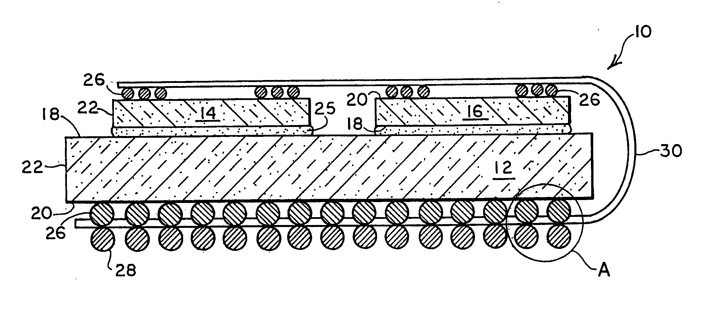
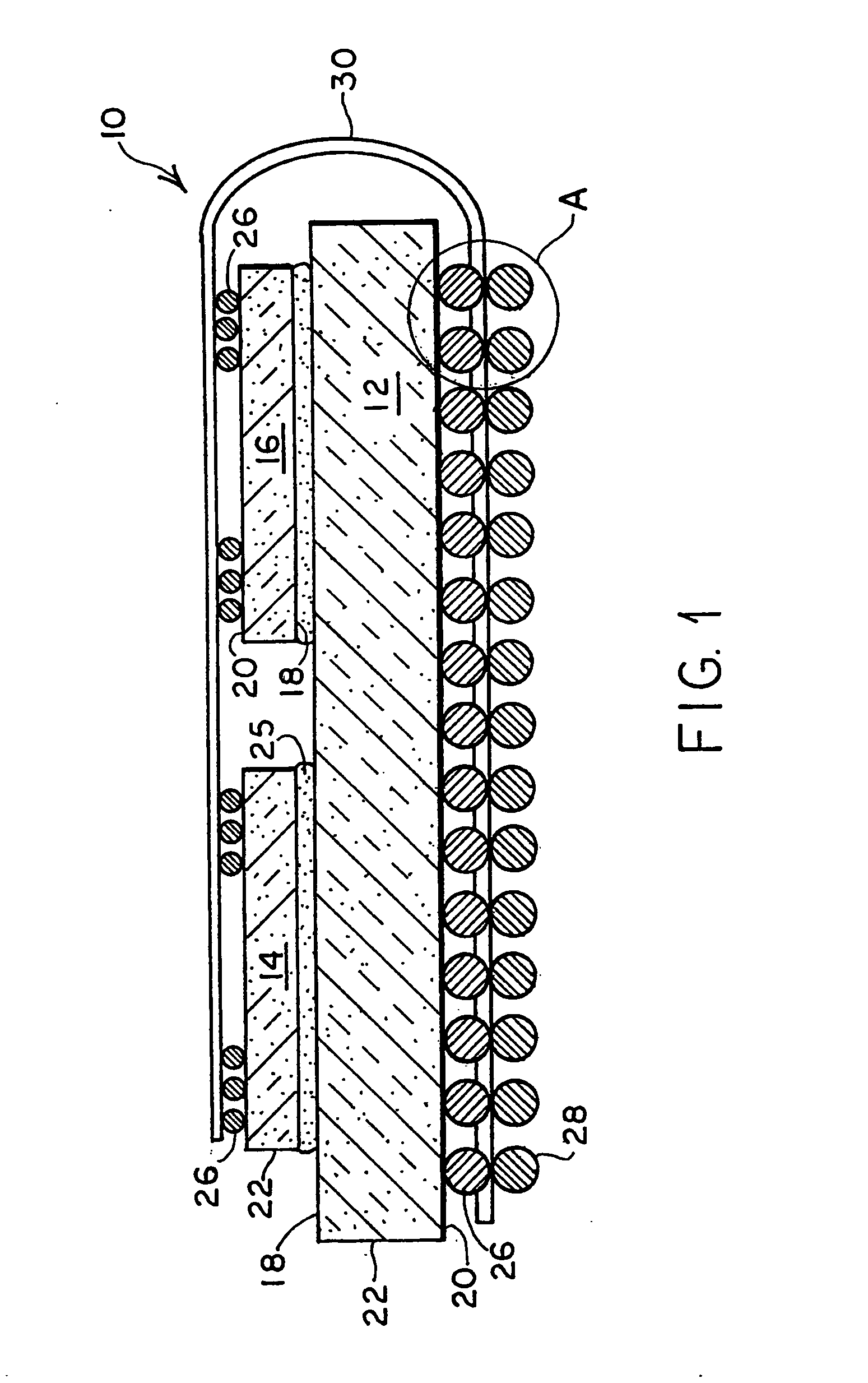
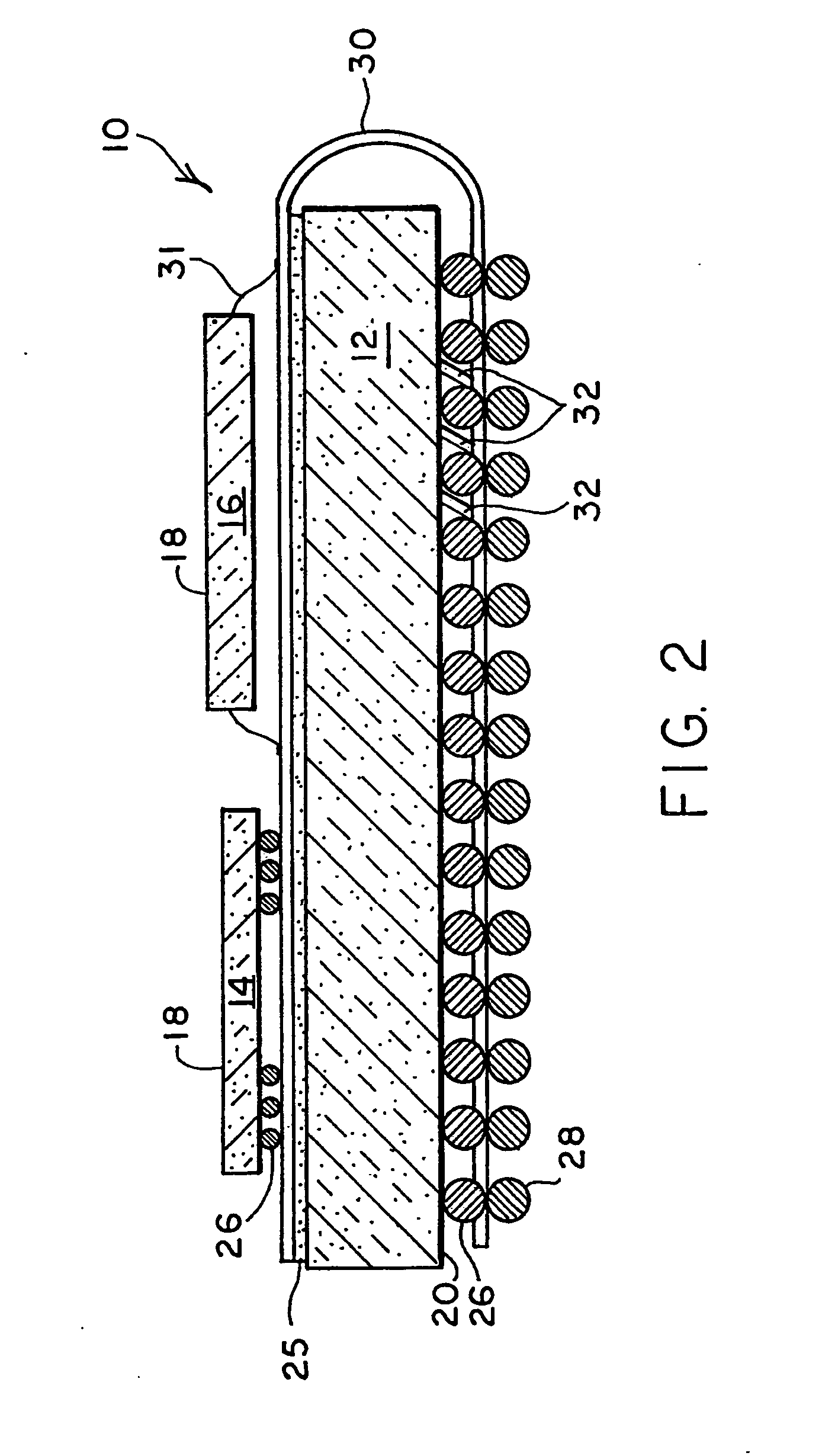
[0033]FIG. 1 is an elevation view of module 10 devised in accordance with a preferred embodiment of the present invention. FIG. 1 depicts a three-element preferred embodiment of the invention. The invention may, however, be employed with greater or fewer than three IC elements. Module 10 is comprised of a base element 12 and support elements 14 and 16. In the depicted embodiment, base element 12 and support elements 14 and 16 are shown as CSP devices, but the invention is not limited to arrangements of CSPs and may be employed to aggregate a variety of package types. Base element 12 and support elements 14 and 16 each have, in the depicted embodiment, upper surfaces 18 and lower surfaces 20 and peripheral or lateral sides 22. Lateral sides 22 may be in the character of sides or may, if the CSP is especially thin, be in the character of an edge. For example, in addition to the well known leaded and CSP packages, the present invention may be employed with packaged ICs that do not exhi...


PUM


Abstract

The present invention stacks packaged integrated circuits into modules that conserve PWB or other board surface area. The present invention can be used to advantage with packages of a variety of sizes and configurations ranging from larger packaged base elements having many dozens of contacts to smaller packages such as, for example, die-sized packages such as DSBGA. In a preferred embodiment devised in accordance with the present invention, a base element CSP integrated circuit and a support element CSP integrated circuit are aggregated through a flex circuit having at least two conductive layers that are patterned to selectively connect the two CSP elements. A portion of the flex circuit connected to the support element is folded over the base element to dispose the support element above the base element while reducing the overall footprint. The flex circuit provides a thermal and electrical connection path between the module and an application environment such as a printed wiring board (PWB).

Description

RELATED APPLICATIONS [0001] This application is a continuation of U.S. app. Ser. No 10 / 136,890, filed May 2, 2002, pending; which is a continuation-in-part of U.S. app. Ser. No. 10 / 005,581, filed Oct. 26, 2001, now U.S. Pat. No. 6,576,992 B1, issued Jun. 10, 2003. U.S. Pat. No. 6,576,992 B1 is hereby incorporated by reference for all purposes.TECHNICAL FIELD [0002] The present invention relates to aggregating integrated circuits and, in particular, to stacking dissimilar integrated circuits. packages. In some stacks, the leads of the packaged integrated circuits are used to create a stack, while in other systems, added structures such as rails provide all or part of the interconnection between packages. In still other techniques, flexible conductors with certain characteristics are used to selectively interconnect packaged integrated circuits. [0003] One major package configuration employed during the past decade has encapsulated an integrated circuit (IC) in a plastic surround typi...

Claims


Application Information

Patent Timeline
Patent Type & Authority Applications(United States)
IPC IPC(8): H01L23/31H01L23/498H01L23/538H01L25/065H01L25/10H05K1/14H05K1/18H05K3/36
CPCH01L23/3114H01L23/49816H01L2224/73253H01L2224/73204H01L2224/32245H01L23/49827H01L23/4985H01L23/5387H01L25/0657H01L25/105H01L2224/16237H01L2225/06517H01L2225/06541H01L2225/06579H01L2225/06586H01L2924/19041H01L2924/3011H05K1/141H05K1/147H05K1/189H05K3/363H05K2201/056H05K2201/10689H05K2201/10734H01L2225/107H01L2225/1094H01L2224/16225H01L2224/32145H01L2224/32225H01L2924/00012
Inventor CADY, JAMES W.WILDER, JAMESROPER, DAVID L.RAPPORT, RUSSELLWEHRLY, JAMES DOUGLAS JR.BUCHLE, JEFFREY ALAN
Owner ENTORIAN TECH L P FORMERLY STAKTEK GROUP
Why Eureka
Try Eureka