Optical interference display panel and manufacturing method thereof

a technology of optical interference and display panel, which is applied in the direction of positive displacement liquid engine, fluid speed measurement, chemical vapor deposition coating, etc., can solve the problems of inability to properly function, inability to detect the light source, and very thin light-reflection electrode, etc., to achieve the effect of lowering the display performance and improving the problem

Active Publication Date: 2005-02-24
QUALCOMM INC +1
View PDF68 Cites 311 Cited by
  • Summary
  • Abstract
  • Description
  • Claims
  • Application Information

AI Technical Summary

Benefits of technology

[0014] In consideration of the foregoing problems, the invention provides a protection structure adhered to the substrate, such that the color-changeable pixels are protectively enclosed to improve the problems. However, if the sacrificial layer used during manufacturing is removed before adhering the protection structure to the substrate, the color-changeable pixel produced by the processing sequence slightly mitigates these problems but cannot substantially avoid them. Since the color-changeable pixel is exposed to air during the period between the sacrificial layer being removed and the protection structure being adhered, water, dust and oxygen in the air are still able to affect the color-changeable pixel and lower its display performance.

Problems solved by technology

Thus, the incident visible light with the wavelength λ2 is absorbed, and the light with other wavelengths has destructive interference.
The light-reflection electrode is very thin and is easily damaged by even a tiny external force, inhibiting it from functioning properly.
The depth D of the cavity is typically less than 1 μm, and therefore the adsorbed water generates an undesirable electrostatic attraction between the two electrodes.
Additionally, the two thin walls 102 and 104 are easily oxidized by air to such an extent that their optical or electrical properties are adversely affected.
However, if the sacrificial layer used during manufacturing is removed before adhering the protection structure to the substrate, the color-changeable pixel produced by the processing sequence slightly mitigates these problems but cannot substantially avoid them.
Since the color-changeable pixel is exposed to air during the period between the sacrificial layer being removed and the protection structure being adhered, water, dust and oxygen in the air are still able to affect the color-changeable pixel and lower its display performance.

Method used


Image

  • Optical interference display panel and manufacturing method thereof
  • Optical interference display panel and manufacturing method thereof
  • Optical interference display panel and manufacturing method thereof

Examples


Embodiment Construction

[0040] Reference will now be made in detail to the present preferred embodiments of the invention, examples of which are illustrated in the accompanying drawings. Wherever possible, the same reference numbers are used in the drawings and the description to refer to the same or like parts.

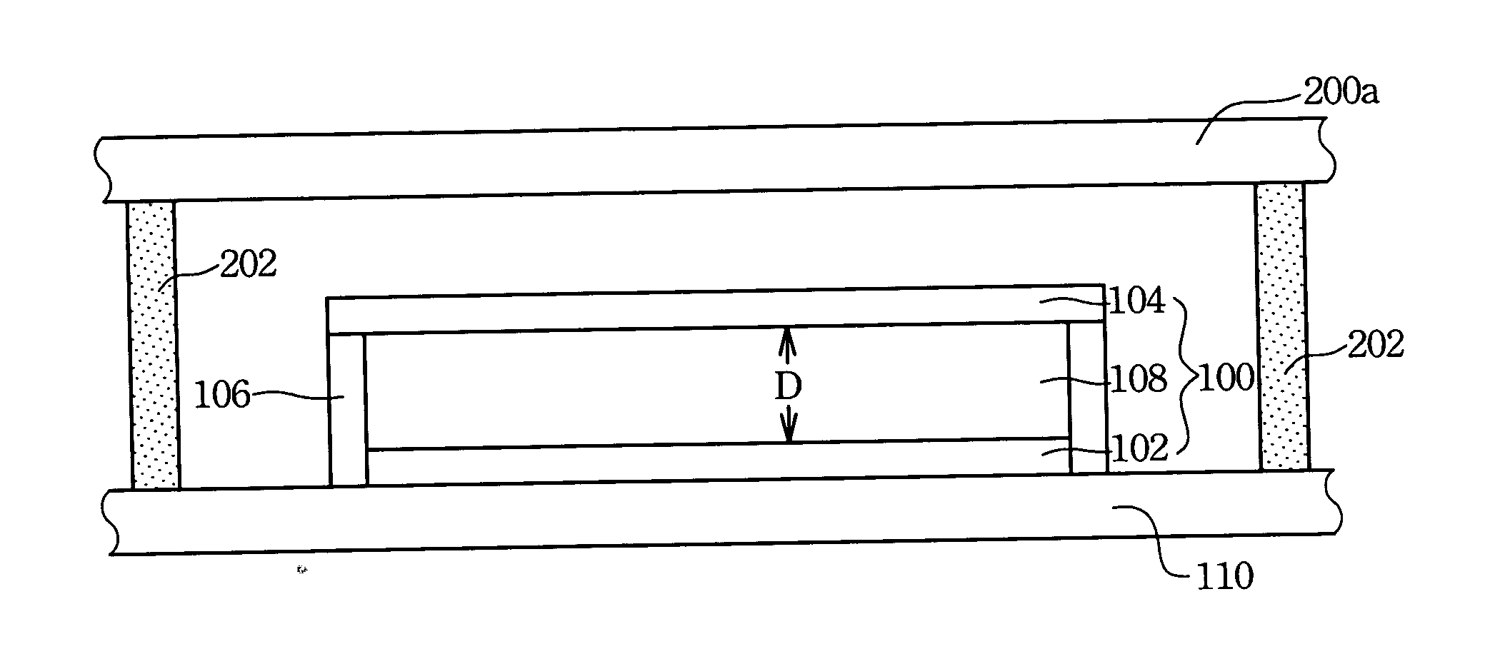
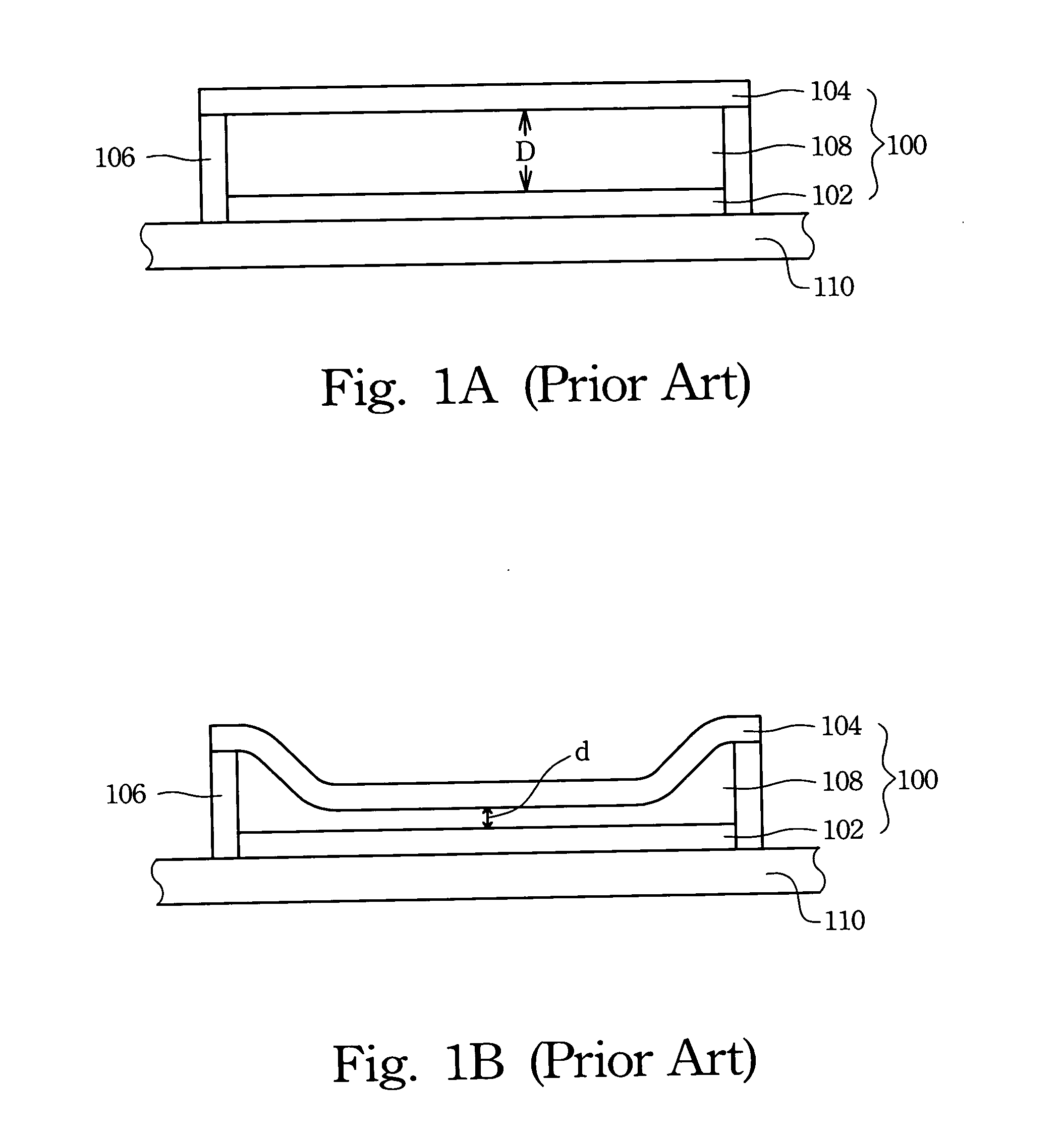
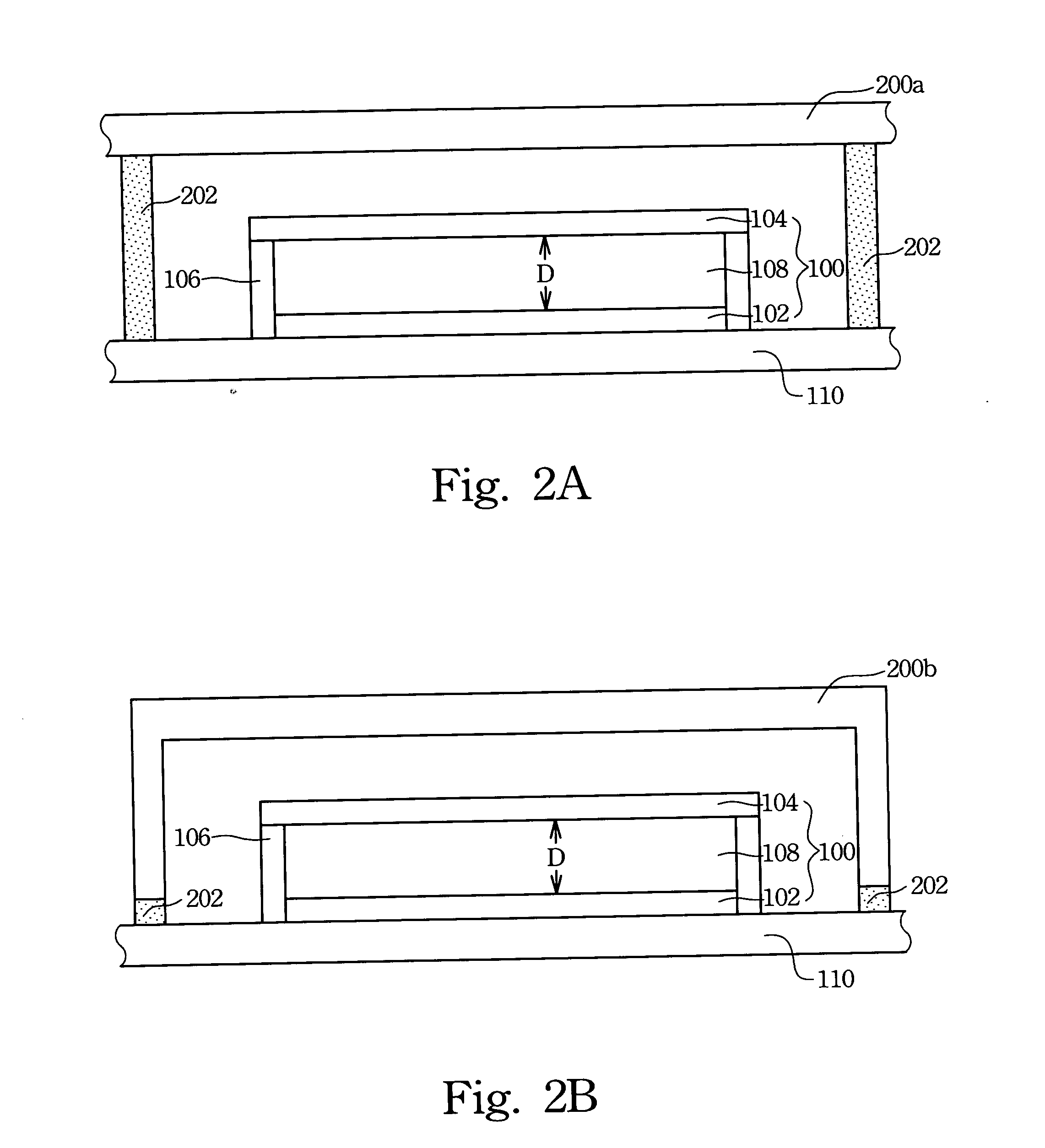
[0041] The manufacturing method of the invention first forms a first electrode and a sacrificial layer in order on the substrate, and then a plurality of first openings are formed in the first electrode and the sacrificial layer. One support is formed in each of the first openings, and a second electrode is then formed on the sacrificial layer and the supports, thus creating a micro electro mechanical structure.

[0042] Next, a protection structure is adhered to the substrate with an adhesive in order to form a chamber which encloses the micro electro mechanical structure therein such that at least one second opening is available on the sidewall of the chamber. A release etching process is then perf...


PUM

PropertyMeasurementUnit
depthaaaaaaaaaa
sizeaaaaaaaaaa
sizeaaaaaaaaaa

Abstract

A first electrode and a sacrificial layer are sequentially formed on a substrate, and then first openings for forming supports inside are formed in the first electrode and the sacrificial layer. The supports are formed in the first openings, and then a second electrode is formed on the sacrificial layer and the supports, thus forming a micro electro mechanical system structure. Afterward, an adhesive is used to adhere and fix a protection structure to the substrate for forming a chamber to enclose the micro electro mechanical system structure, and at least one second opening is preserved on sidewalls of the chamber. A release etch process is subsequently employed to remove the sacrificial layer through the second opening in order to form cavities in an optical interference reflection structure. Finally, the second opening is closed to seal the optical interference reflection structure between the substrate and the protection structure.

Description

BACKGROUND [0001] 1. Field of Invention [0002] The present invention relates to a display panel. More particularly, the present invention relates to an optical interference display panel. [0003] 2. Description of Related Art [0004] Due to being lightweight and small in size, a display panel is favorable in the market of portable displays and other displays with space limitations. To date, in addition to liquid crystal display (LCD), organic light emitting diode (OLED) and plasma display panel (PDP) modules, a module of the optical interference display has been investigated. [0005] U.S. Pat. No. 5,835,255 discloses a modulator array, that is, a color-changeable pixel for visible light which can be used in a display panel. FIG. 1A illustrates a cross-sectional view of a prior art modulator. Every modulator 100 comprises two walls, 102 and 104. These two walls are supported by posts 106, thus forming a cavity 108. The distance between these two walls, the depth of cavity 108, is D. The...

Claims


Application Information

Patent Timeline
Patent Type & Authority Applications(United States)
IPC IPC(8): B81B3/00B81B7/00G02B26/08B81B7/02B81C1/00F04B37/02F04F99/00G02B26/00G09F9/00G09F9/30
CPCB81B7/0012G02B26/001B81B2201/045G02B26/08
Inventor LIN, WEN-JIAN
Owner QUALCOMM INC
Why Eureka
Try Eureka