Dual salicide process for optimum performance

a dual-suicide, optimal performance technology, applied in the direction of semiconductor/solid-state device manufacturing, basic electric elements, electric apparatus, etc., can solve the problems of personal devices requiring more computational power and speed, and achieve high-efficiency manufacturing, high-efficiency processing, and high-efficiency effects

Active Publication Date: 2005-02-24
TEXAS INSTR INC
View PDF8 Cites 20 Cited by
  • Summary
  • Abstract
  • Description
  • Claims
  • Application Information

AI Technical Summary

Benefits of technology

[0009] The present invention pertains to forming respective salicides on multiple transistors in a single process. High performance is facilitated with simple and highly integrated process flows. As such, transistors and an integrated circuit containing the transistors can be fabricated efficiently and at a low cost. The different salicides can be formed with different materials and / or to different thicknesses. The salicides can, accordingly, have different electrical characteristics, such as resistivity and conductivity, and thus instill the transistors with different work functions when formed as gate contacts on the transistors. This provides an integrated circuit containing the transistors with diverse operating capabilities allowing for more flexibility and / or functionality.

Problems solved by technology

In addition to being smaller and more portable, personal devices are requiring more computational power and speed.

Method used


Image

  • Dual salicide process for optimum performance
  • Dual salicide process for optimum performance
  • Dual salicide process for optimum performance

Examples


Embodiment Construction

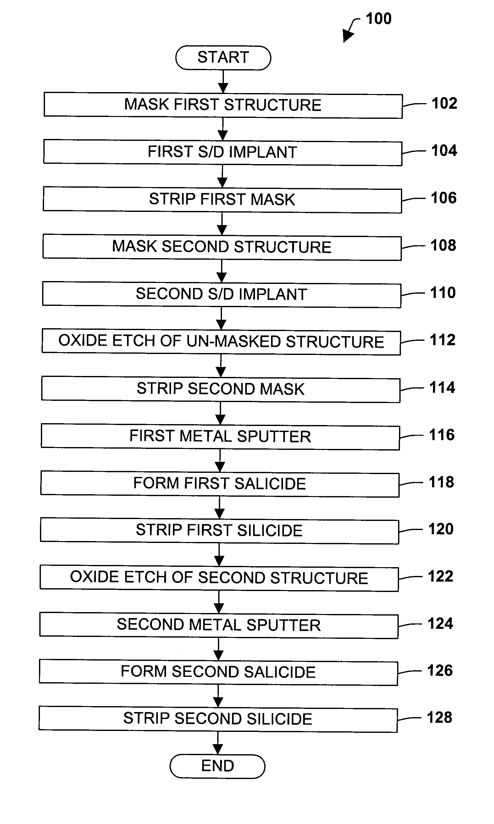
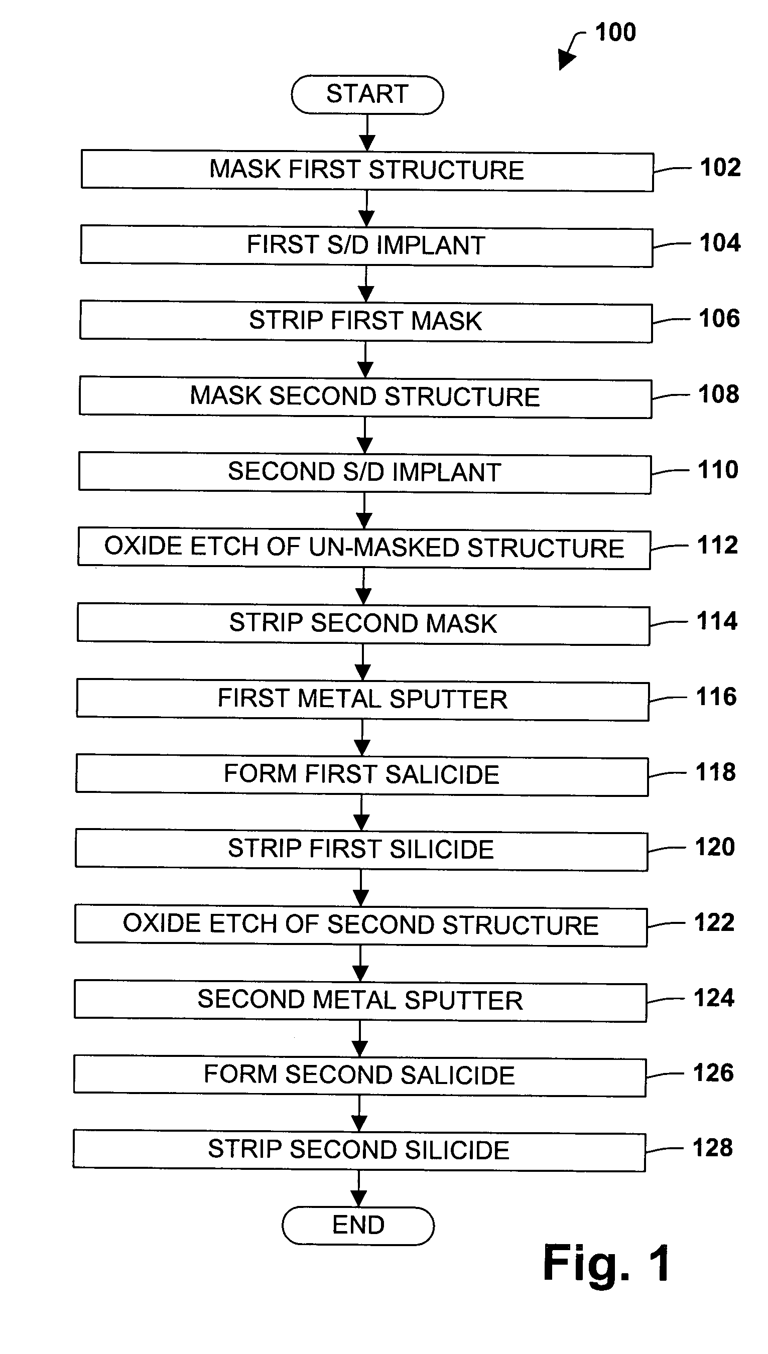
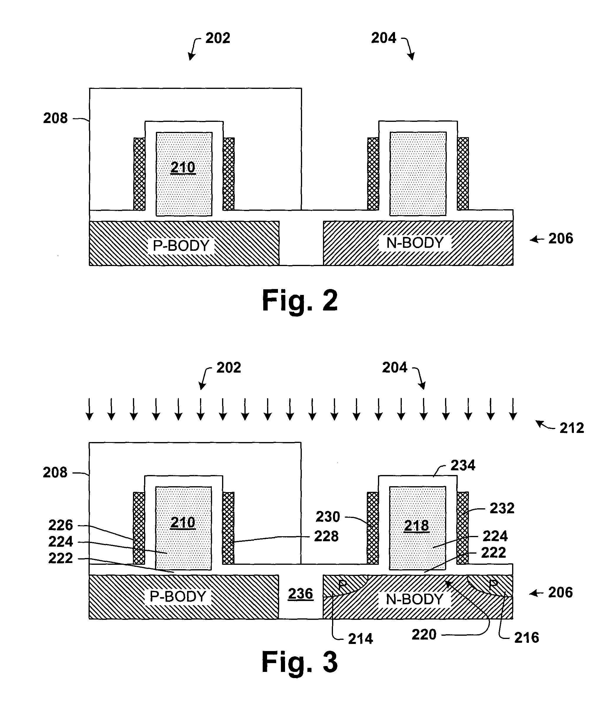
[0015] One or more aspects of the present invention are described with reference to the drawings, wherein like reference numerals are generally utilized to refer to like elements throughout, and wherein the various structures are not necessarily drawn to scale. In the following description, for purposes of explanation, numerous specific details are set forth in order to provide a thorough understanding of one or more aspects of the present invention. It may be evident, however, to one skilled in the art that one or more aspects of the present invention may be practiced with a lesser degree of these specific details. In other instances, well-known structures and devices are shown in block diagram form in order to facilitate describing one or more aspects of the present invention.

[0016] One or more aspects of the present invention pertain to forming respective salicides on multiple transistors in a single process. High device performance is facilitated with simple and highly integrat...


PUM


Abstract

The present invention pertains to forming respective suicides on multiple transistors in a single process. High performance is facilitated with simple and highly integrated process flows. As such, transistors, and an integrated circuit containing the transistors, can be fabricated efficiently and at a low cost. The different suicides can be formed with different materials and / or to different thicknesses. As such, the silicides can have different electrical characteristics, such as resistivity and conductivity. These different attributes instill the transistors with different work functions when formed as gate contacts thereon. This provides an integrated circuit containing the transistors with diverse operating capabilities allowing for the execution of operations requiring more flexibility and / or functionality.

Description

FIELD OF INVENTION [0001] The present invention relates generally to semiconductor processing, and more particularly to an efficient dual suicide process. BACKGROUND OF THE INVENTION [0002] Several trends exist presently in the semiconductor and electronics industry. Devices are continually getting smaller, faster and requiring less power. A reason for these trends is that more personal devices are being fabricated that are relatively small and portable, thereby relying on a battery as their primary supply source. For example, cellular phones, personal computing devices, and personal sound systems are devices in great demand in the consumer market. In addition to being smaller and more portable, personal devices are requiring more computational power and speed. In light of all these trends, there is an ever increasing demand in the industry for smaller and faster transistors used to provide the core functionality of the integrated circuits used in these devices. [0003] Accordingly, ...

Claims


Application Information

Patent Timeline
Patent Type & Authority Applications(United States)
IPC IPC(8): H01L21/8238
CPCH01L21/823814H01L21/823864H01L21/823835
Inventor MEHROTRA, MANOJ
Owner TEXAS INSTR INC
Why Eureka
Try Eureka