
Structure and manufacturing process of a nano device transistor for a biosensor

a biosensor and nano-device technology, applied in thermoelectric devices, biomass after-treatment, instruments, etc., can solve the problems of easy misjudgment, too large dependence on the stability of the manufacturing process, and difficult control of the uniformity of the practical impurity doping concentration,

Active Publication Date: 2005-03-03
IND TECH RES INST
View PDF9 Cites 15 Cited by
  • Summary
  • Abstract
  • Description
  • Claims
  • Application Information

AI Technical Summary

Benefits of technology

[0010] The present invention relates to a structure and manufacturing process of a nano device transistor for a biosensor. The structure, the manufacturing process and the related circuit for a nano device transistor for a biosensor are provided. The refurbished carbon nano tube and nano wire are used for absorbing various anti-bodies so as to detect the specific antigens or absorbing various biotins. Therefore, the object to detect the specific species for bio measurement can be achieved.

Problems solved by technology

Therefore, when the number of the bio objects to be detected, which are absorbed on the surface, the misjudgment is easily happened.
However, the dependence on the stability of the manufacturing process is too great, and it is not easy to control the uniformity of the practical impurity doping concentration.
Therefore, the conduction characteristic of the device will be affected.
However, the above methods are not effective, and the results are not good.

Method used


Image

  • Structure and manufacturing process of a nano device transistor for a biosensor
  • Structure and manufacturing process of a nano device transistor for a biosensor
  • Structure and manufacturing process of a nano device transistor for a biosensor

Examples


Embodiment Construction

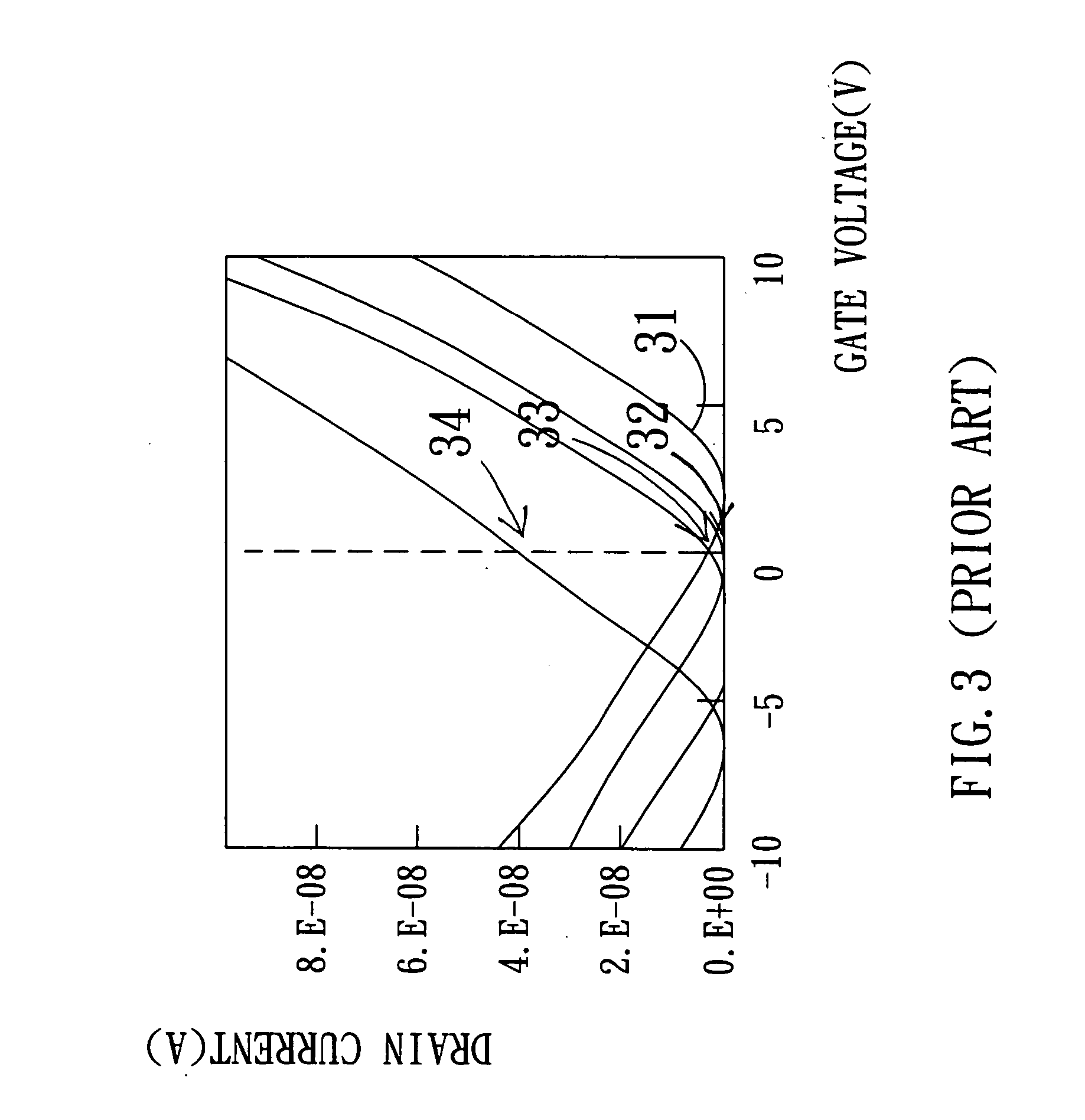
[0020] Because the carbon nano tube and the nano wire device transistor for the bio and chemical sensor having the characteristic of the two-way conduction, the misjudgment will be easily caused when the number of the bio and chemical objects to be detected which are absorbed on the surface of the nano device are varied. Therefore, the present invention provides an off-set nano device transistor having the characteristic of one-way conduction. Even though the number of the bio objects to be detected which are absorbed on the surface of the nano device are different, the variation trend of the detection current varies in the same direction. This makes the misjudgment not easily happen.

[0021] Please refer to FIG. 4A to FIG. 4F. FIG. 4A to FIG. 4F are perspective diagrams for the manufacturing process of an off-set nano device transistor. As shown in FIG. 4A, a bottom gate layer 42 is deposited on a silicon substrate 41 having SiO2 deposited on it. This bottom gate layer 42 can be mad...


PUM

PropertyMeasurementUnit
gate voltageaaaaaaaaaa
areaaaaaaaaaaa
dielectricaaaaaaaaaa

Abstract

The present invention relates to a structure and manufacturing process of a nano device transistor for a biosensor. The structure, the manufacturing process and the related circuit for a carbon nano tube or nano wire transistor biosensor device are provided. The refurbished nano device is used for absorbing various anti-bodies so as to detect the specific antigens or absorbing various biotins. Therefore, the object of the present invention to detect the specific species for bio measurement can be achieved.

Description

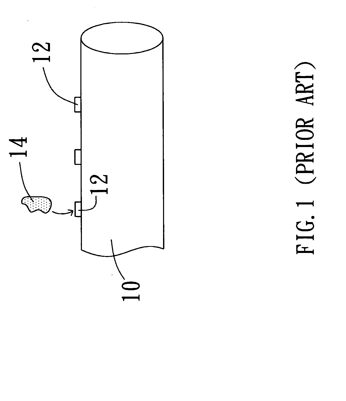
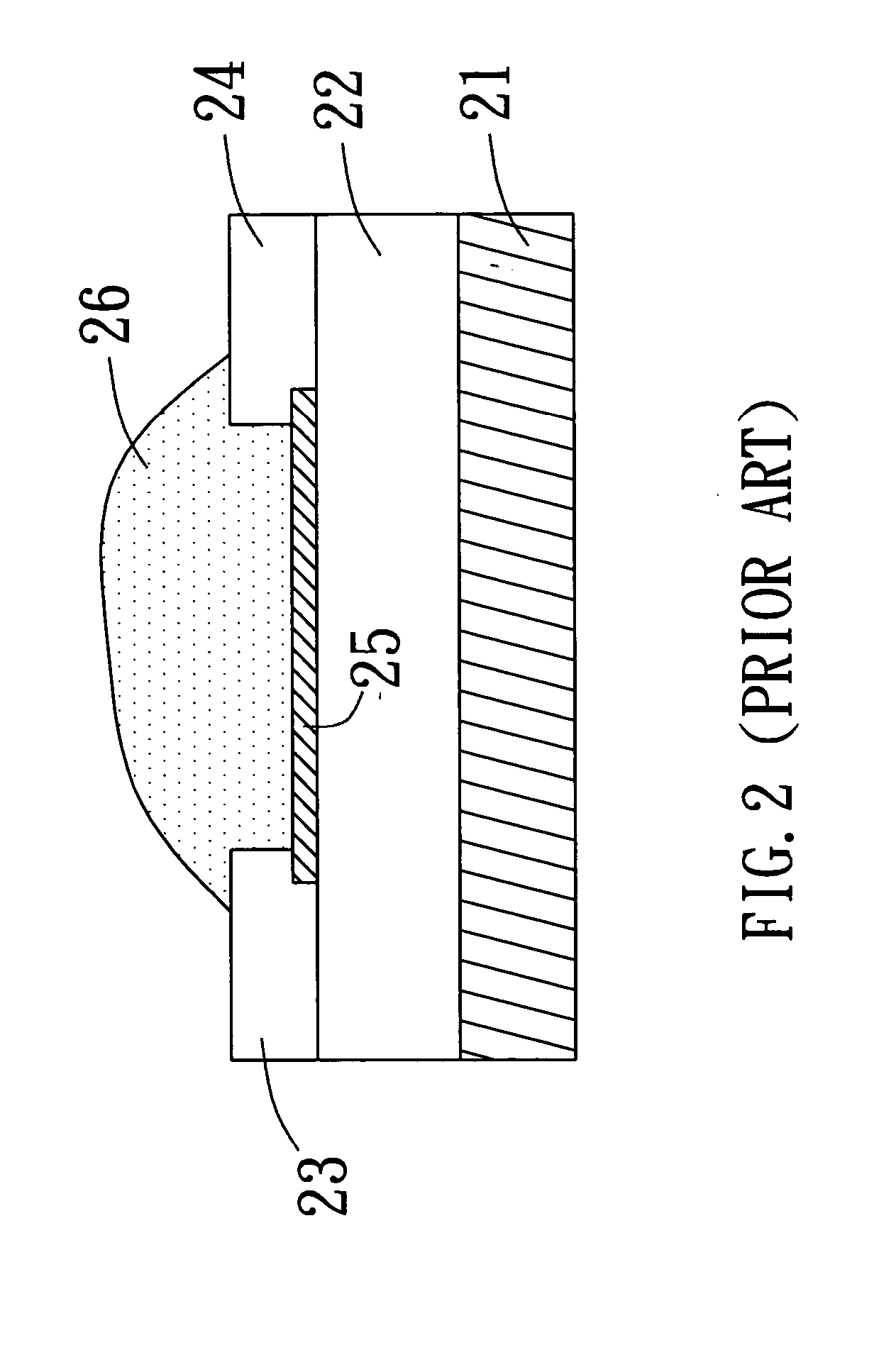
BACKGROUND OF THE INVENTION [0001] 1. Field of the Invention [0002] The present invention relates to a structure, manufacturing process and related circuit for a nano device transistor for a biosensor so as to achieve the object of detecting the specific species for bio measurement. [0003] 2. Description of the Prior Art [0004] In the journal of “Science” published in 2001, Professor Charles M. Lieber, the professor of the chemical department of Harvard university, published a paper related to the manufacturing of the biological and chemical sensor by using nano wire. As shown in FIG. 1, the refurbished nano wire 10 is used for absorbing different anti-bodies 12. After the antigen 14 and the anti-body 12 are combined and absorbed on the surface of the nano wire, the relative polarization (dipole) effect of the electric charges in the molecule on the nano wire 10 is equivalent to the effect of forming a fixed bias on the surface of the nano wire. This bias will affect the energy band...

Claims


Application Information

Patent Timeline
Patent Type & Authority Applications(United States)
IPC IPC(8): G01N27/414
CPCB82Y5/00B82Y15/00G01N27/4146H10K19/10H10K10/466
Inventor LAI, MING-JIUNNWANG, HUNG-HSIANGWEI, JENG-HUACHEN, HSIN-HUIKAO, MING-JER
Owner IND TECH RES INST
Learn More