Flip chip stacked package

a technology of flip chip and stacking package, which is applied in the direction of semiconductor devices, semiconductor/solid-state device details, electrical apparatus, etc., can solve the problems of poor thermal performance of the package and the size of the package will increase, so as to enhance enhance the heat dissipation capability. , the effect of upgrading the thermal performance of the packag

Active Publication Date: 2005-03-03
ADVANCED SEMICON ENG INC
View PDF6 Cites 39 Cited by
  • Summary
  • Abstract
  • Description
  • Claims
  • Application Information

AI Technical Summary

Benefits of technology

[0010] In view of the above-mentioned problems, the invention is to provide a flip chip stacked package with the enhanced capability of heat dissipation so as to upgrade the thermal performance of said package.
[0011] To achieve the above-mentioned, a flip chip stacked package is provided, wherein the flip chip stacked package mainly comprises a carrier, such as a substrate, an upper chip, a lower chip, a plurality of bumps, a plurality of bonding wires, and a supporter. Therein, the carrier has an opening; and the supporter is disposed under the opening and attached to the carrier through an adhesive so as to cover the opening. Besides, the lower chip is disposed above the supporter and the upper chip is attached to the lower chip through the bumps. In addition, each bump has a adequate height so as to have the upper chip wire bonding to the su...

Problems solved by technology

Accordingly, said heat is not directly transmitted to the outside and the therma...

Method used


Image

  • Flip chip stacked package
  • Flip chip stacked package
  • Flip chip stacked package

Examples


Embodiment Construction

[0018] The flip chip stacked package according to the preferred embodiments of this invention will be described herein below with reference to the accompanying drawings, wherein the same reference numbers refer to the same elements.

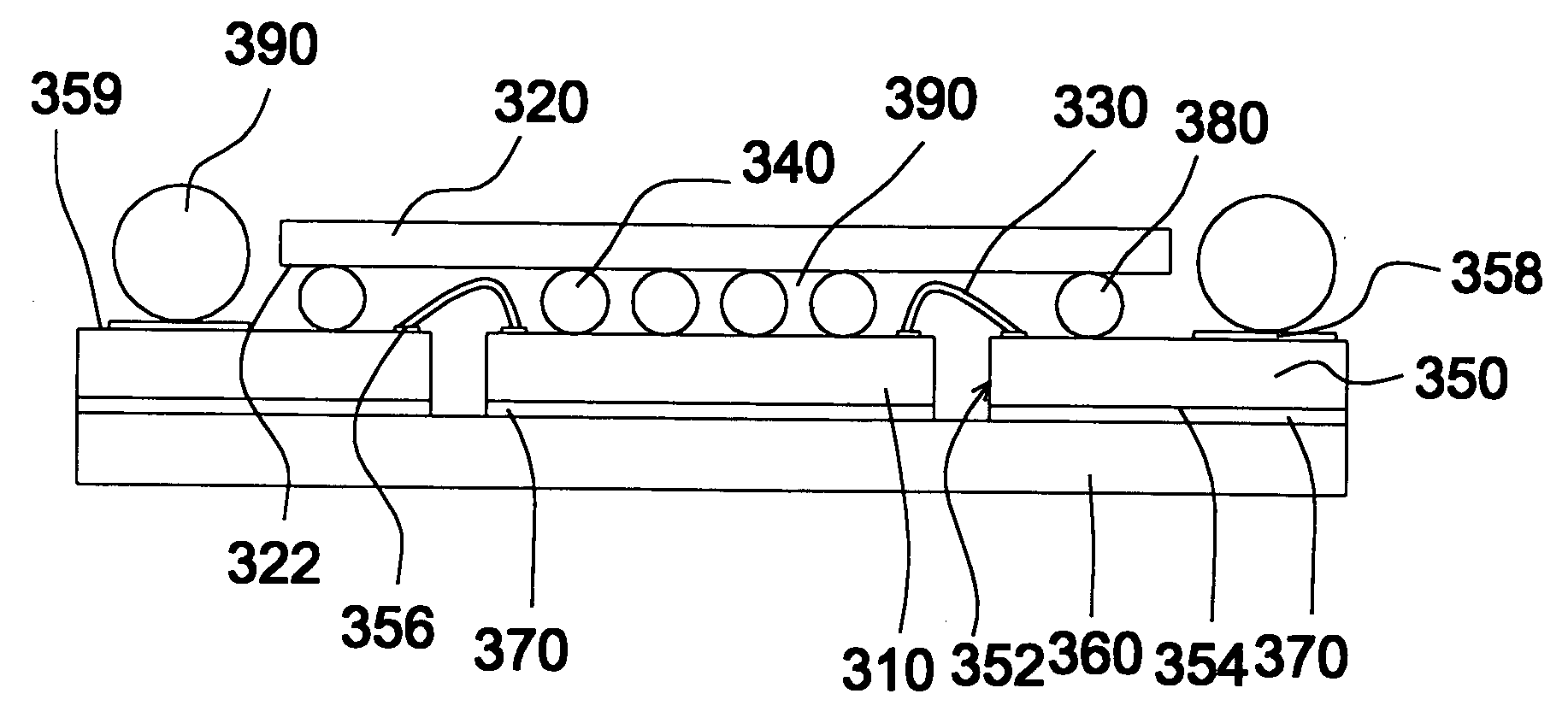
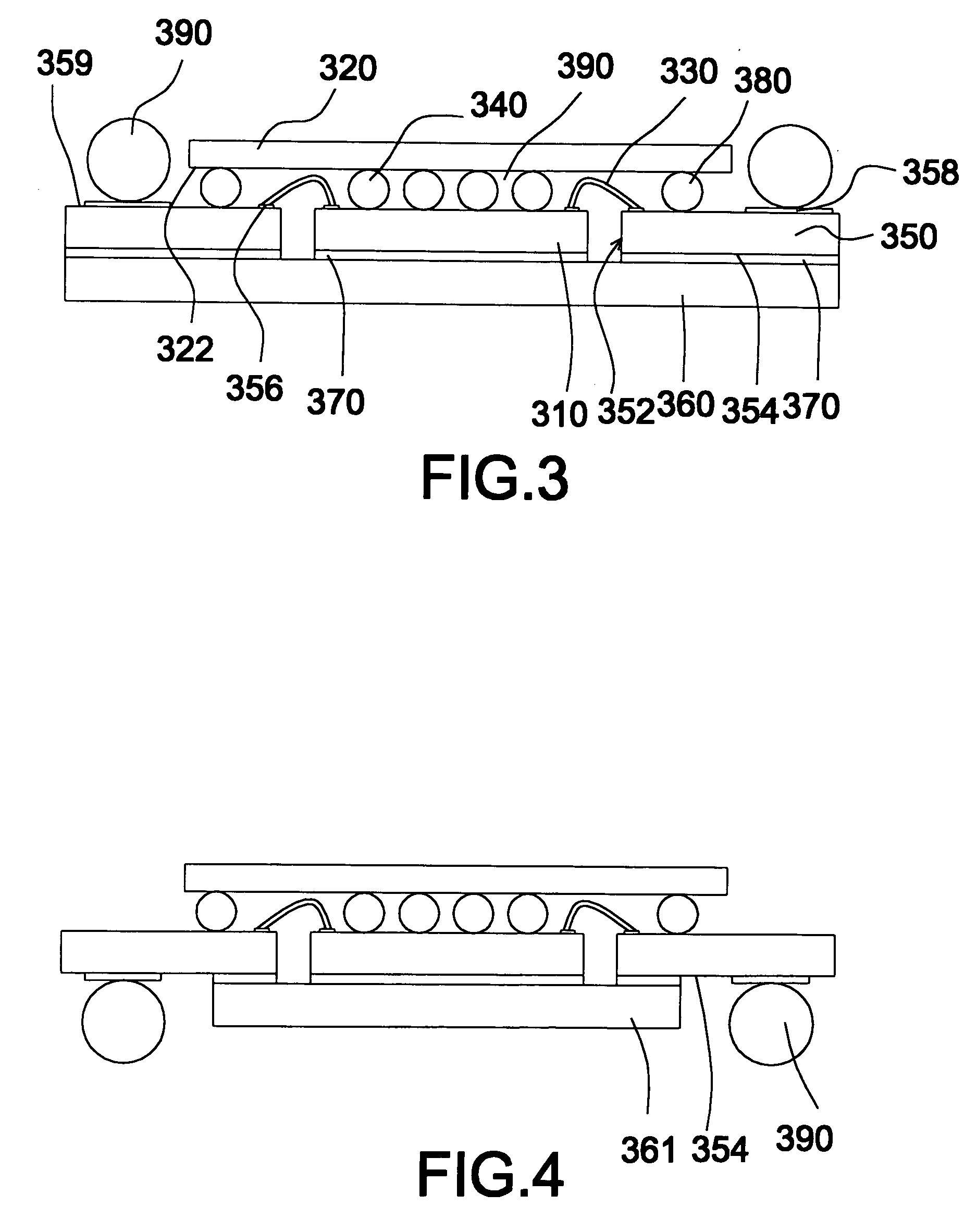
[0019] In accordance with a first preferred embodiment as shown in FIG. 3, there is provided a flip chip stacked package. The flip chip stacked package mainly comprises a lower chip 310, an upper chip 320, a plurality of bonding wires 330, a plurality of bumps 340, a carrier 350 and a supporter 360. Therein, the supporter 360 is disposed below the opening 352 of the carrier 350 and attached to the lower surface 354 of the carrier 350 through an adhesive 370 so as to carry the lower chip 310 and have the lower chip 310 accommodated in the opening 352. Besides, the lower chip 310 is electrically connected to the upper chip 320 through the bumps 340 so as to have the lower chip 310 flip-chip bonded to the upper chip 320. Moreover, each of the bumps 340 has ...


PUM


Abstract

A flip chip stacked package mainly comprises a carrier, a lower chip, an upper chip, a plurality of bumps, a plurality of bonding wires and a supporter. The supporter is attached to the lower surface of the carrier via an adhesive and covers the opening of the carrier. Thus, the lower chip can be disposed in the opening. In addition, the lower chip is electrically flip-chip bonded to the upper chip via the bumps and electrically connected to the carrier via the bonding wires. Accordingly, the heat generated from the lower chip can be transmitted to outside via the supporter. Furthermore, the upper chip is directly exposed to outside so that the capability of the heat dissipation will be enhanced.

Description

BACKGROUND OF THE INVENTION [0001] 1. Field of Invention [0002] This invention relates to a flip chip stacked package. More particularly, the present invention is related to a flip chip stacked package with the enhanced capability of heat dissipation so as to upgrade the thermal performance of said package. [0003] 2. Related Art [0004] In this information explosion age, integrated circuits products are used almost everywhere in our daily life. As fabricating technique continue to improve, electronic products having powerful functions, personalized performance and a higher degree of complexity are produced. Nowadays, most electronic products are relatively light and have a compact body. Hence, in semiconductor production, various types of high-density semiconductor packages have been developed. Flip chip is one of the most commonly used techniques for forming an integrated circuits package. Moreover, compared with a wire-bonding package or a tape automated bonding (TAB) package, a fl...

Claims


Application Information

Patent Timeline
IPC IPC(8): H01L25/065
CPCH01L24/73H01L25/0657H01L2924/10253H01L2224/45144H01L2924/01033H01L2224/16145H01L2224/48227H01L2224/73207H01L2225/0651H01L2225/06513H01L2225/06517H01L2225/06555H01L2225/06586H01L2924/01029H01L2924/01079H01L2924/14H01L2924/15311H01L2924/1532H01L2924/01005H01L2924/00H01L2924/181
Inventor WANG, SUNG-FEIHO, MING-LUN
Owner ADVANCED SEMICON ENG INC
Why Eureka
Try Eureka