Rolling contact screening method and apparatus

a contact screening and roller technology, applied in the direction of resistive material coating, liquid/solution decomposition chemical coating, superimposed coating process, etc., can solve the problems of high electrical resistance, strain and wear of stencil masks, and achieve sufficient friction and prevent slippage of rollers

Inactive Publication Date: 2005-03-17
IBM CORP
View PDF15 Cites 12 Cited by
  • Summary
  • Abstract
  • Description
  • Claims
  • Application Information

AI Technical Summary

Benefits of technology

[0015] A further aspect of the present invention provides an apparatus for applying paste to an electronic circuit board substrate comprising, a mask for an electronic circuit board substrate, the mask having discrete openings therein for forming structures on the substrate, a roller having an axis and a surface adjacent the roller and the mask, and a paste applicator for applying paste to a side of the surface facing the mask. The roller and the surface containing the paste are adapted to roll over the mask and flow the paste into the openings in the mask and on to the substrate without substantially sliding the roller and surface over the mask.
[0016] Preferably, the surface is on a film strip and the apparatus further includes at least one spool for feeding the film strip between the roller and the mask after paste is applied thereto. The surface is preferably made of a plastic that does not substantially absorb components of the paste, while having sufficient friction to substantially prevent slippage of the roller during rolling over the mask and flowing of the paste into the mask openings.

Problems solved by technology

Such silk screening methods have had difficulty in filling vias, and the generally lower line heights result in higher electrical resistance.
While these nozzle application methods have been successful, there is a certain amount of strain and wear on the stencil mask as a result of the contact pressures required.

Method used


Image

  • Rolling contact screening method and apparatus
  • Rolling contact screening method and apparatus
  • Rolling contact screening method and apparatus

Examples


Embodiment Construction

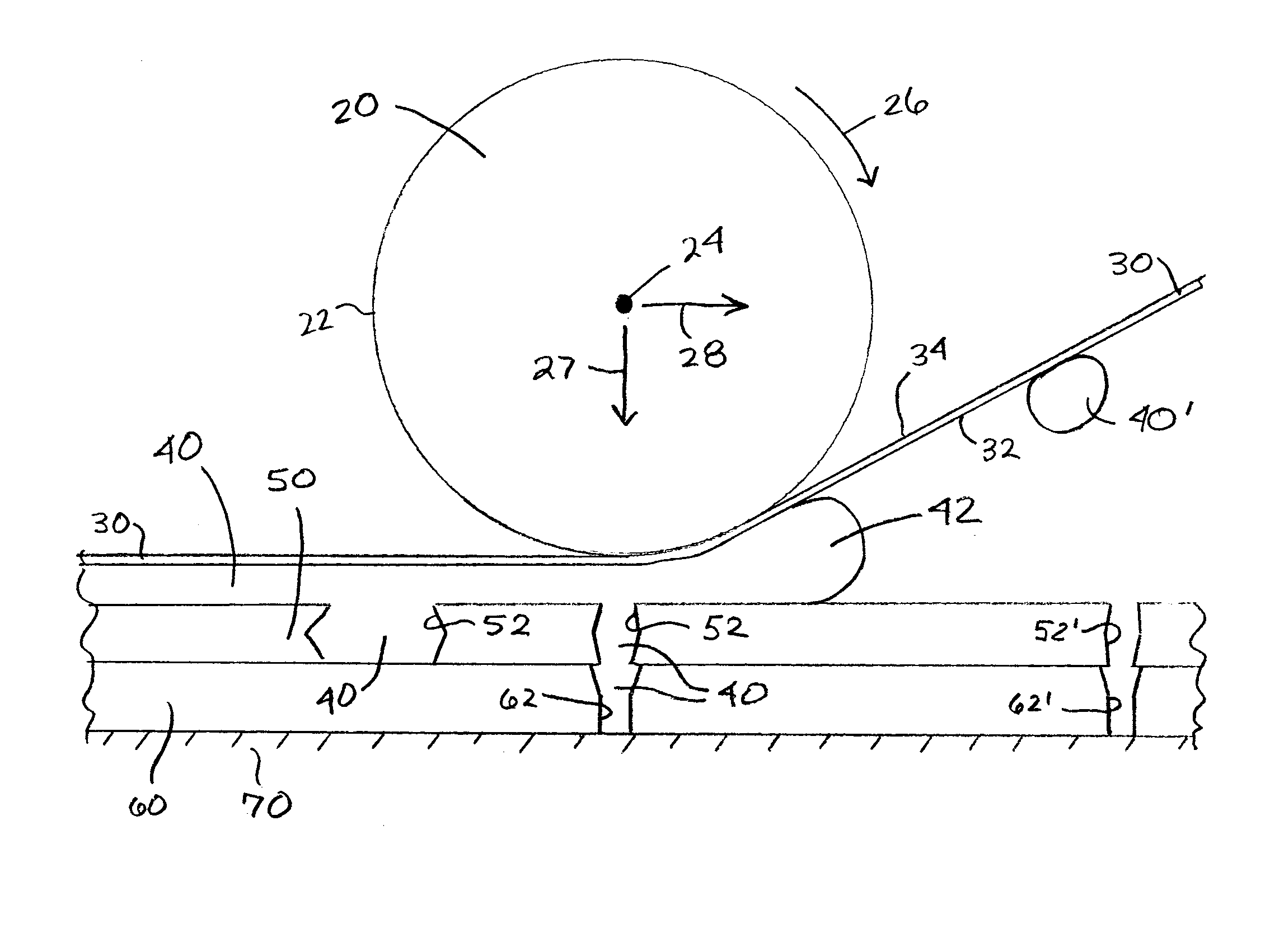
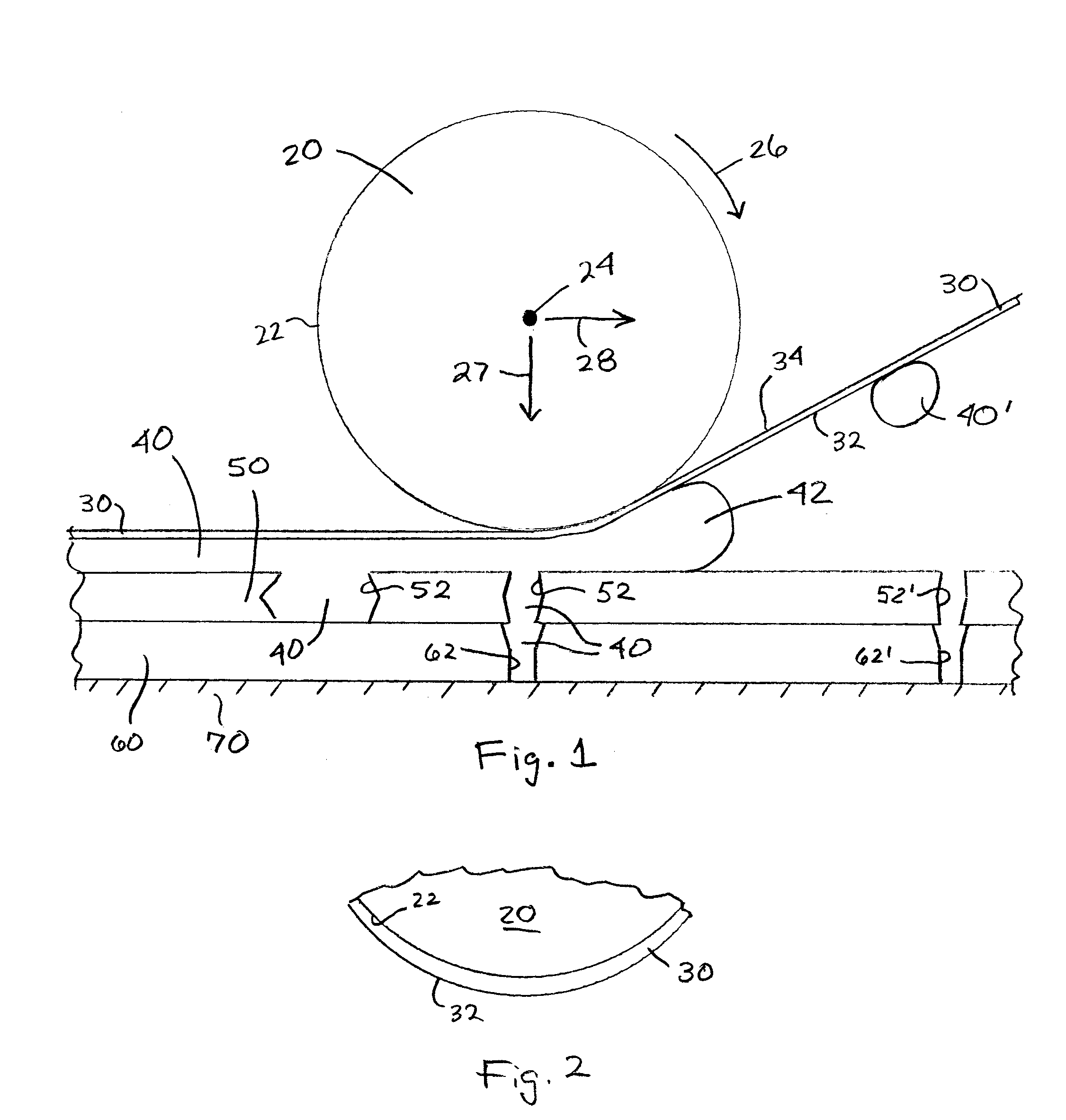
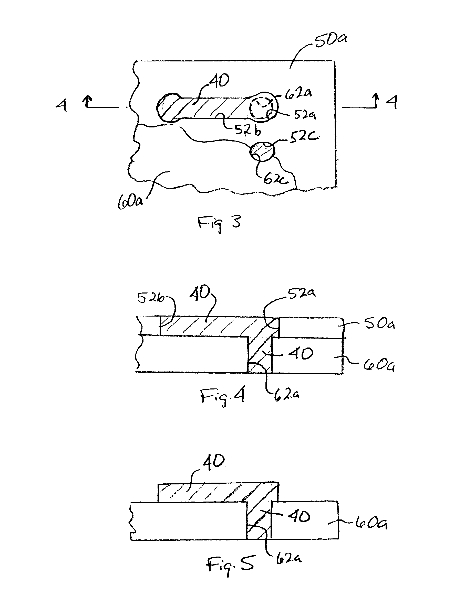
[0030] In describing the preferred embodiment of the present invention, reference will be made herein to FIGS. 1-9 of the drawings in which like numerals refer to like features of the invention.

[0031] The preferred apparatus and method of the present invention simultaneously screens lines and fills vias while maintaining purely rolling contact with the screening or stencil mask utilized over the printed circuit board substrate. The basic features of the method and apparatus are depicted in FIG. 1 in which a workpiece fixture 70 has mounted thereon a single layer of a printed circuit board substrate 60 and, directly thereover, stencil mask 50. Substrate 60 has discrete, spaced-apart openings 62, 62′ therein and mask 50 has corresponding openings 52, 52′ respectively aligned with the substrate openings. The purpose of the stencil mask openings is to permit conductive paste to be forced into the stencil mask openings only, and to form the desired conductive lines on the substrate surf...


PUM

PropertyMeasurementUnit
speedaaaaaaaaaa
velocitiesaaaaaaaaaa
widthaaaaaaaaaa

Abstract

A method of applying paste to an electronic circuit board substrate containing via openings comprises providing over the substrate a mask having openings therein for lines and openings corresponding to the substrate via openings, and providing a roller having a surface adjacent the roller. Paste is then applied either to the mask or to a side of the surface facing the mask. The method then includes rolling the roller and the surface over the mask and flowing the paste into the openings in the mask without substantially sliding the roller and surface over the mask. In the preferred embodiment, paste is applied to a side of the surface facing the mask and the surface containing the paste is rolled over the mask. The surface may be attached to the roller. More preferably, the surface is on a film strip, separate from the roller, disposed between the roller and the substrate.

Description

BACKGROUND OF INVENTION [0001] 1. Field of the Invention [0002] This invention relates to the manufacture of electronic circuit boards and, in particular, to a method and apparatus for rolling contact screening of conductive pastes through stencil masks to create lines and vias in circuit board substrates. [0003] 2. Description of Related Art [0004] Printed circuit boards utilized in high-density electronic applications have utilized organic, i.e., epoxy and fiberglass, or ceramic, i.e., sintered green sheets, substrates which contain conductive lines, vias and other structures. Lines are deposited on the surface of the substrate, and vias are created in holes which are aligned through two or more layers of the substrate. The conductive lines are manufactured by screening a conductive paste onto the surface of the substrate and then curing the paste; the conductive vias are manufactured by filling the via openings with a conductive paste and then curing the paste. Prior art methods ...

Claims


Application Information

Patent Timeline
Patent Type & Authority Applications(United States)
IPC IPC(8): B41F15/42H05K3/12H05K3/40
CPCB41F15/42H05K2203/0143H05K3/4053H05K3/1233
Inventor HERRON, L. WYNNHUMENIK, JAMES N.LONG, DAVID C.MILLER, JASON S.
Owner IBM CORP
Why Eureka
Try Eureka