Micro-lens configuration for small lens focusing in digital imaging devices

a digital imaging device and micro-lens technology, applied in the direction of discharge tubes/lamp details, instruments, photoelectric discharge tubes, etc., can solve the problems of difficult to tailor fabrication techniques to produce micro-lenses, additional processing effort, expense and time,

Active Publication Date: 2005-03-24
APTINA IMAGING CORP
View PDF7 Cites 54 Cited by
  • Summary
  • Abstract
  • Description
  • Claims
  • Application Information

AI Technical Summary

Benefits of technology

[0013] The present invention provides micro-lenses formed to focus light onto the photo sensors of the image sensor such that the depth of the photo sensors does not have to be decreased even when the image sensor device, including its photo sensors and micro-lenses, decrease in size.
[0022] The use of a sacrificial material in the present invention allows fabrication of micro-lenses of a desired focal length such that light may be directed to corresponding photo sensors at a desired depth in a semiconductor substrate.
[0023] The geometry of the micro-lenses fabricated using the sacrificial material lens molds can be formed to a variety of shapes. Preferably, the micro-lenses formed according to the invention have a concave shape. Concave micro-lenses may provide improved light capture, such as for example where the edges of the micro-lenses of a given micro-lens array touch or overlap in the surface plane of the array.

Problems solved by technology

Decreasing the photo sensor's depth in the substrate, however, requires manufacturing changes, and results in additional effort, expense and time in processing.
These fabrication techniques are difficult to tailor to produce micro-lenses that direct light to a particular focal point when the micro-lens size and geometry (and resultant focal length) change.
Additionally, in known image sensors, a large amount of light incident on the image sensor device is not directed to the photo sensor due to the geometry of the micro-lens array.
It is difficult to produce image sensor micro-lenses with improved light capture using known patterning and micro-lens reflow processes.
This passivation layer causes undesirable reflection in the optical path to the photo sensors.

Method used


Image

  • Micro-lens configuration for small lens focusing in digital imaging devices
  • Micro-lens configuration for small lens focusing in digital imaging devices
  • Micro-lens configuration for small lens focusing in digital imaging devices

Examples


Embodiment Construction

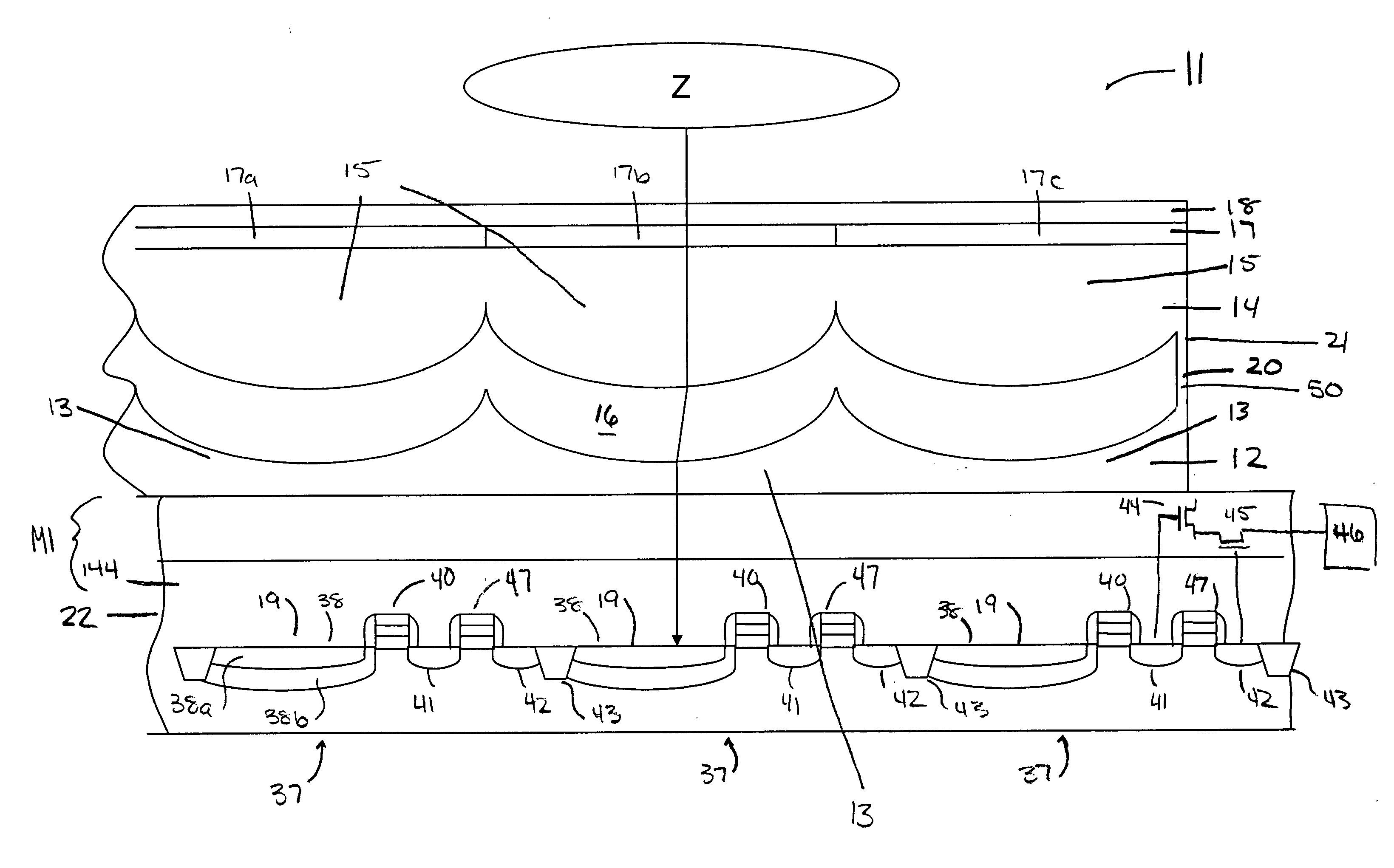
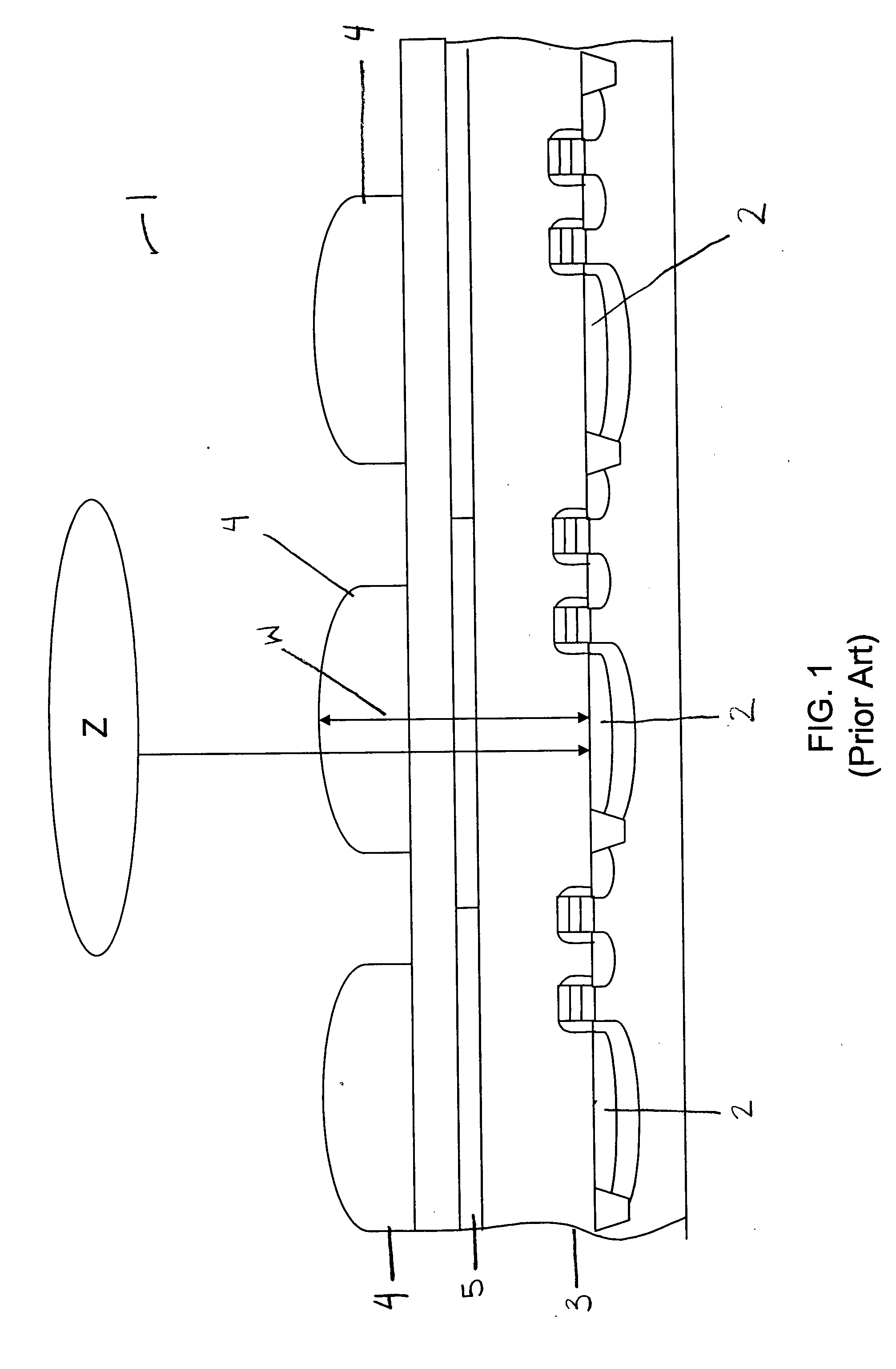
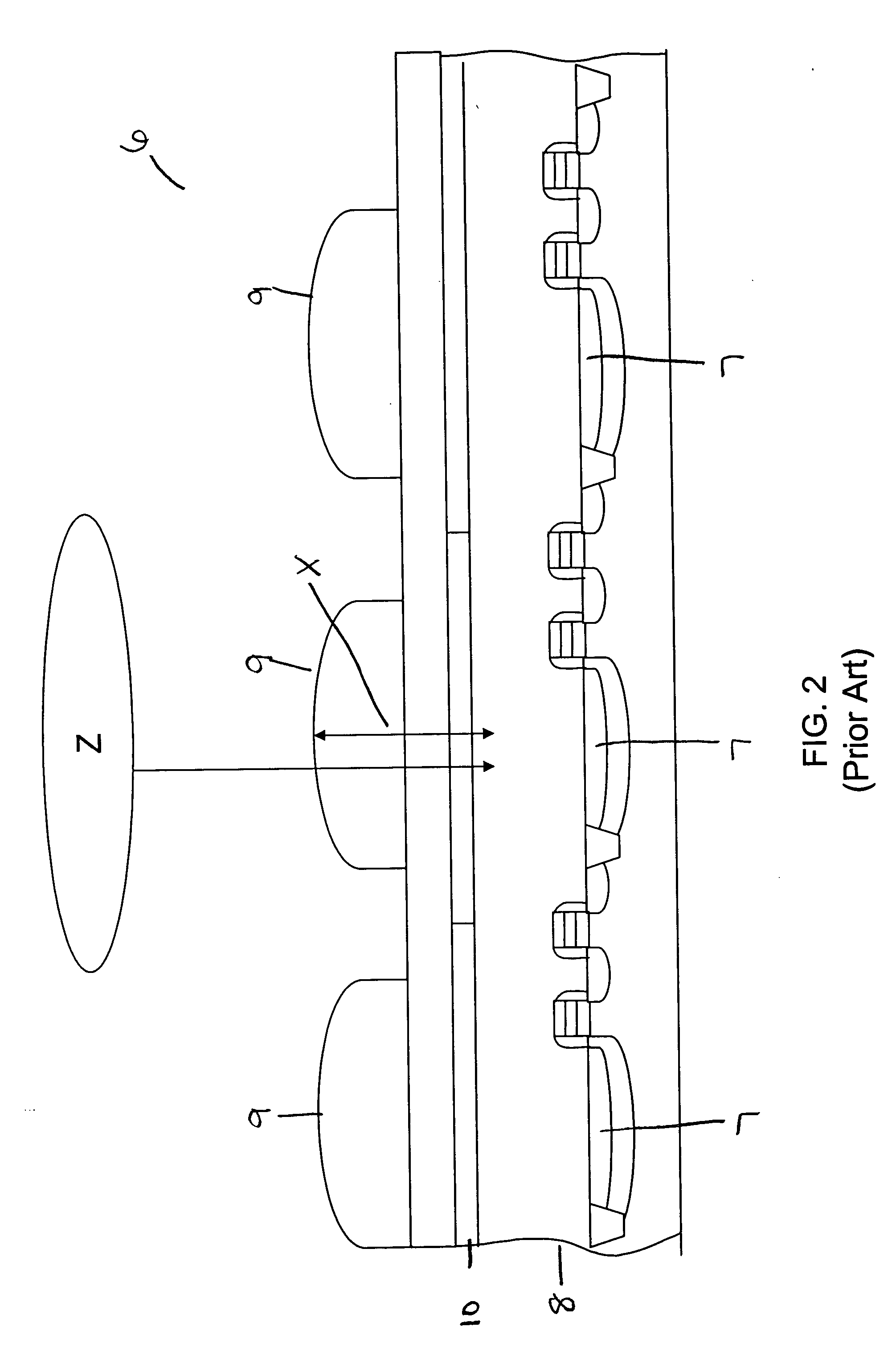
[0061] In the following detailed description, reference is made to the accompanying drawings which form a part hereof, and which illustrate specific embodiments of the present invention. These embodiments are described in sufficient detail to enable those of ordinary skill in the art to make and use the invention. It is also understood that structural, logical, or procedural changes may be made to the specific embodiments disclosed without departing from the spirit and scope of the present invention.

[0062] The terms “wafer” and “substrate” are to be understood as interchangeable and as including silicon, silicon-on-insulator (SOI) or silicon-on-sapphire (SOS), doped and undoped semiconductors, epitaxial layers of silicon supported by a base semiconductor foundation, and other semiconductor structures. Furthermore, when reference is made to a “wafer” or “substrate” in the following description, previous process steps may have been utilized to form regions, junctions or material laye...


PUM


Abstract

An improved image sensor wherein a first micro-lens array comprised of one pr more micro-lenses is positioned over a cavity such that incoming light is focused on the photo sensors of the image sensor. The first micro-lens array may collimate and focus incoming light onto the photo sensors of the image sensor, or may collimate incoming light and direct it to a second micro-lens array which then focuses the light onto the photo sensors. A method of fabricating the improved image sensor id also provided wherein the cavity and first micro-lens array are formed by use of a sacrificial material.

Description

BACKGROUND OF THE INVENTION [0001] 1. Field of the Invention [0002] The present invention relates generally to micro-lenses for imager devices and to methods for producing the same. [0003] 2. Brief Description of the Related Art [0004] Image sensing devices (i.e., image sensors) are known that employ light detecting elements (e.g., photo sensors) for use in various applications such as in semiconductor devices. Such image sensors may be formed using a variety of fabrication techniques. Currently, two commonly fabricated image sensors are CMOS image sensors and charge coupled device (CCD) image sensors. Each generally includes an array of pixels containing the photo sensors. The image sensors typically use photo sensors in the form of photogates, phototransistors or photodiodes. [0005] When an image is focused on the imager array, light corresponding to the image is directed to the pixels, including the photo sensors. It is known in the art to use an imager array of pixels having a m...

Claims


Application Information

Patent Timeline
Patent Type & Authority Applications(United States)
IPC IPC(8): H01J3/14H01J5/16H01L27/00
CPCH01L27/14627B33Y80/00
Inventor JIANG, TONGBICONNELL, MICHAELLI, JIN
Owner APTINA IMAGING CORP
Why Eureka
Try Eureka