Image sensor having global and rolling shutter processes for respective sets of pixels of a pixel array

a technology of image sensor and global shutter, applied in the field of electronic image sensor, can solve the problems of unsatisfactory motion artifacts in the output image, other types of artifacts, and provide any substantial reduction in the generation of rolling shutter artifacts, so as to reduce the generation of motion artifacts and other artifacts, increase the cost or complexity of the imaging device, and reduce the effect of motion artifacts

Inactive Publication Date: 2010-12-09
OMNIVISION TECH INC
View PDF11 Cites 112 Cited by
  • Summary
  • Abstract
  • Description
  • Claims
  • Application Information

AI Technical Summary

Benefits of technology

[0017]An image sensor in accordance with the invention may be advantageously implemented in a digital camera or other type of imaging device, and provides substantial reduc

Problems solved by technology

Although the use of a rolling shutter process avoids the cost and complexity of a mechanical shutter, it can also lead to undesirable motion artifacts in an output image.
The use of a rolling shutter process can also lead to other types of artifacts, such as different rows in a captured image exhibiting different levels of brightness due to different amounts of flash time.
See, for example, U.S. Patent Application Publication No. 2007/0154202, entitled “M

Method used


Image

  • Image sensor having global and rolling shutter processes for respective sets of pixels of a pixel array
  • Image sensor having global and rolling shutter processes for respective sets of pixels of a pixel array
  • Image sensor having global and rolling shutter processes for respective sets of pixels of a pixel array

Examples


Embodiment Construction

[0028]The present invention will be illustrated herein in conjunction with particular embodiments of digital cameras, image sensors, image sensor circuitry and associated image readout techniques. It should be understood, however, that these illustrative arrangements are presented by way of example only, and should not be viewed as limiting the scope of the invention in any way. Those skilled in the art will recognize that the disclosed arrangements can be adapted in a straightforward manner for use with a wide variety of other types of imaging devices, image sensors, image sensor circuitry and associated image readout techniques.

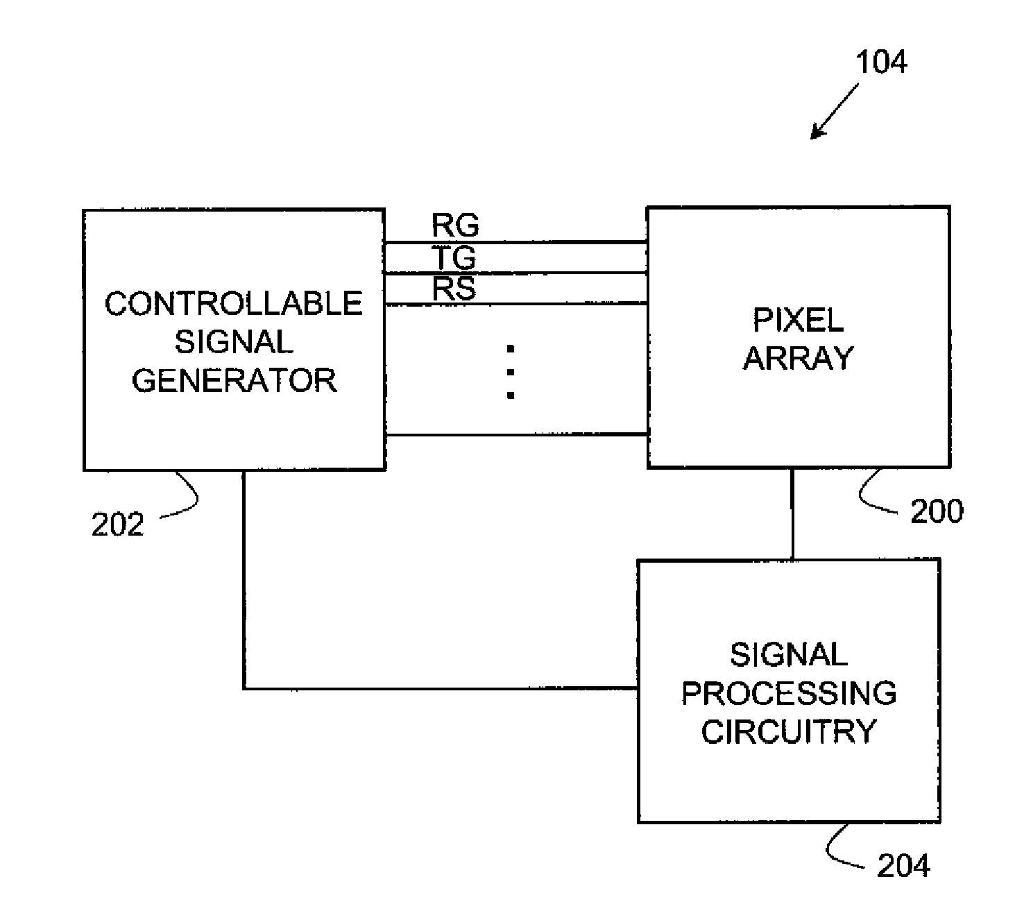
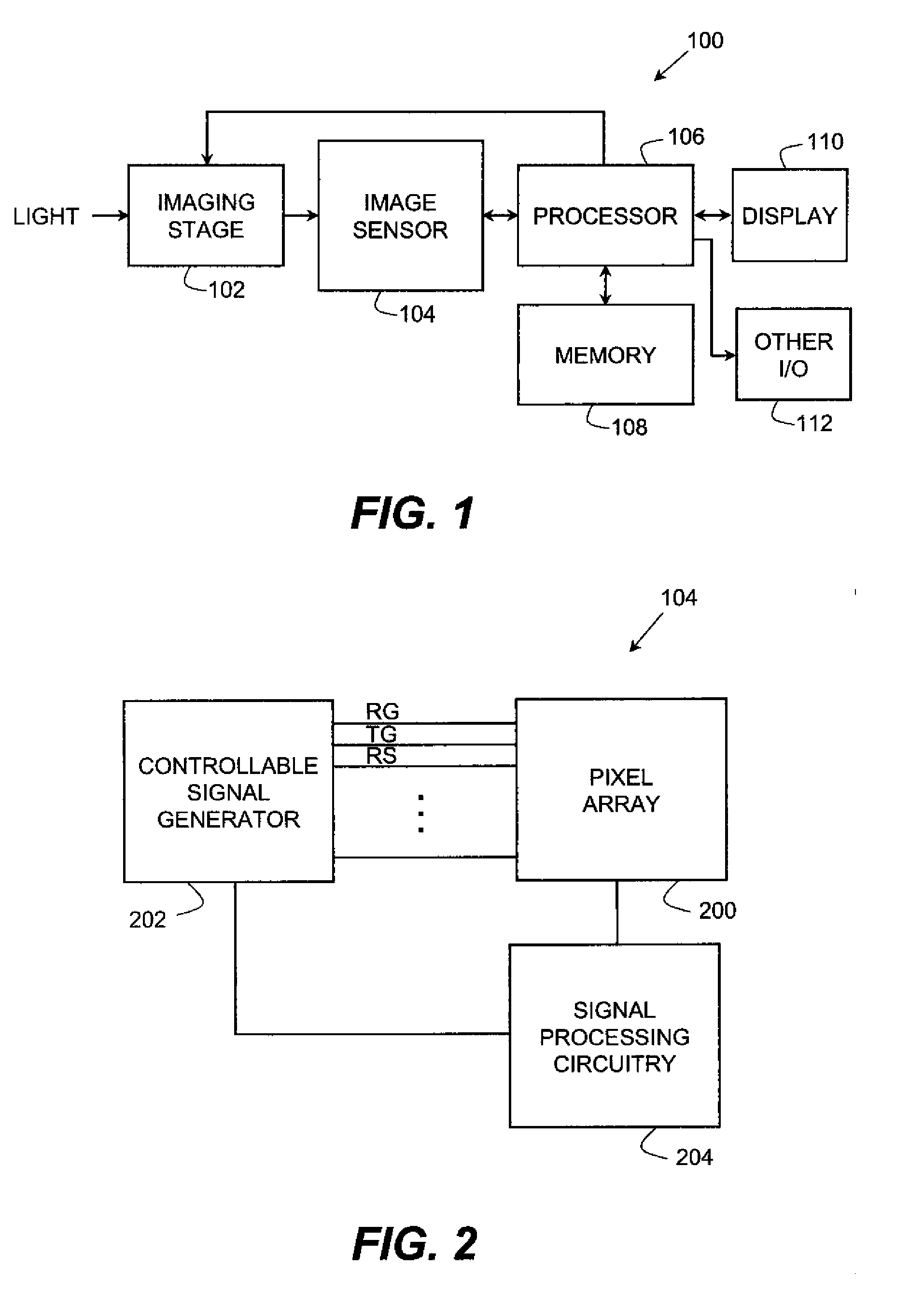
[0029]FIG. 1 shows a digital camera 100 in an illustrative embodiment of the invention. In the digital camera, light from a subject scene is input to an imaging stage 102. The imaging stage may comprise conventional elements such as a lens, a neutral density filter, an iris and a shutter. The light is focused by the imaging stage 102 to form an image on an ...


PUM


Abstract

A CMOS image sensor or other type of image sensor includes a pixel array comprising at least first and second sets of pixels. Image sensor circuitry is coupled to the pixel array and comprises a signal generator for controlling capture of image data from the first set of pixels of the pixel array using a global shutter process and for controlling capture of image data from the second set of pixels of the pixel array using a rolling shutter process, with the pixels of the second set being different than the pixels of the first set The image sensor may be implemented in a digital camera or other type of digital imaging device.

Description

FIELD OF THE INVENTION[0001]The present invention relates generally to electronic image sensors for use in digital cameras and other types of imaging devices, and more particularly to image readout in an electronic image sensor.BACKGROUND OF THE INVENTION[0002]A typical electronic image sensor comprises a number of photodiodes or other photosensitive elements arranged in a two-dimensional array. These elements are also commonly referred to as picture elements or “pixels” and the corresponding array is referred to as a pixel array. Light incident on the pixel array is converted to electrical charge by the photosensitive elements. Collected electrical charge for a given image capture period is read from the photosensitive elements of the pixel array using an active pixel sensor (APS) or charge-coupled device (CCD) arrangement.[0003]As is well known, an APS image sensor may be implemented using complementary metal-oxide-semiconductor (CMOS) circuitry. An image sensor of this type is co...

Claims


Application Information

Patent Timeline
IPC IPC(8): H04N5/335H04N5/217
CPCH04N5/335H04N5/35554H04N5/353H04N25/53H04N25/583H04N25/00
Inventor BORDER, JOHN N.COMPTON, JOHN T.
Owner OMNIVISION TECH INC
Why Eureka
Try Eureka