

Method and apparatus for providing an integrated printed circuit board registration coupon
a technology of printed circuit board and registration coupon, which is applied in the direction of printed element electric connection formation, inspection/indentification of circuits, electrical apparatus contruction details, etc., can solve the problems of dramatic increase in circuit density and complexity, dramatic decrease in power consumption and package size, and compromise of electrical circuit integrity
- Summary
- Abstract
- Description
- Claims
- Application Information
AI Technical Summary
Problems solved by technology
Method used
Image

Examples
Embodiment Construction
[0017] In the following detailed description of the preferred embodiments, reference is made to the accompanying drawings that form a part hereof, and in which are shown by way of illustrating specific embodiments in which the invention can be practiced. The embodiments illustrated are described in sufficient detail to enable those skilled in the art to practice the teachings disclosed herein. Other embodiments can be utilized and derived therefrom, such that structural and logical substitutions and changes can be made without departing from the scope of present inventions. The following detailed description, therefore, is not to be taken in a limiting sense, and the scope of various embodiments of the invention is defined only by the appended claims, along with the full range of equivalents to which such claims are entitled.
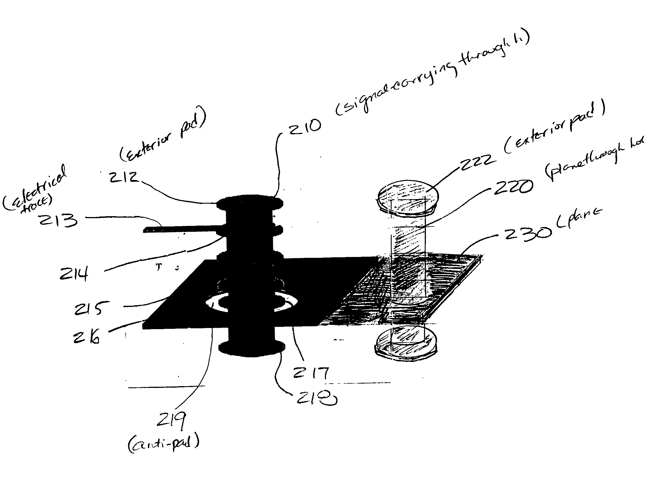
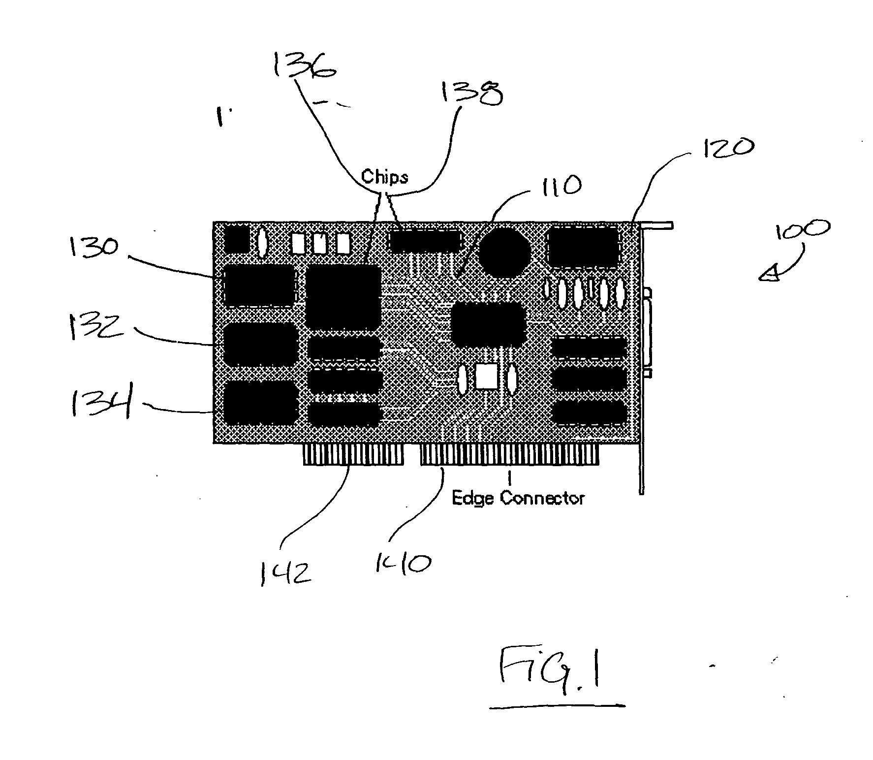
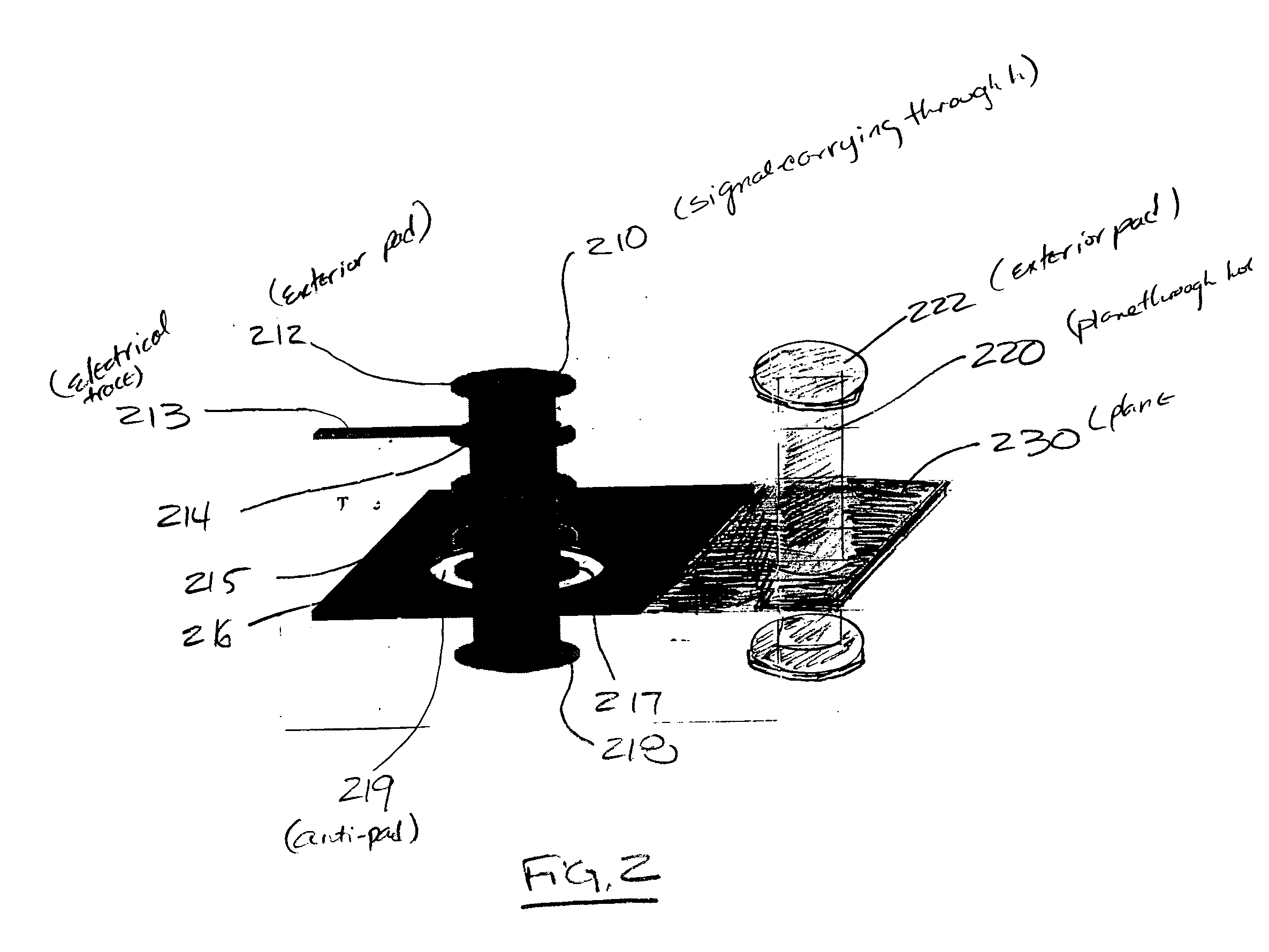
[0018]FIG. 1 is a top view of a printed circuit board 100, according to an embodiment of the invention. The printed circuit board (“PCB”) 100 is a multi-layer ...
PUM
 Abstract
Description
Claims
Application Information