Organic EL panel

a technology of electroluminescence panel and organic el, which is applied in the direction of discharge tube luminescnet screen, identification means, instruments, etc., can solve the problems of reducing the aperture ratio, reducing the service life of organic el elements, and difficult to achieve the appropriate positioning of the driver tft, etc., to achieve the effect of increasing the freedom of arrangement of elements, simplifying the wiring pattern of the gate electrode, and increasing the aperture ratio

Active Publication Date: 2005-04-07
SANYO ELECTRIC CO LTD
View PDF19 Cites 142 Cited by
  • Summary
  • Abstract
  • Description
  • Claims
  • Application Information

AI Technical Summary

Benefits of technology

[0010] According to the present invention, a drive transistor has a substantially L-shaped (L or invert L) semiconductor layer. This can increase freedom in arranging elements o...

Problems solved by technology

However, increase of a current amount results in reduction of the service life of an organic EL element.
With these factors, approp...

Method used


Image

  • Organic EL panel
  • Organic EL panel
  • Organic EL panel

Examples


Embodiment Construction

[0015] In the following, an embodiment of the present invention will be described with reference to the accompanied drawings.

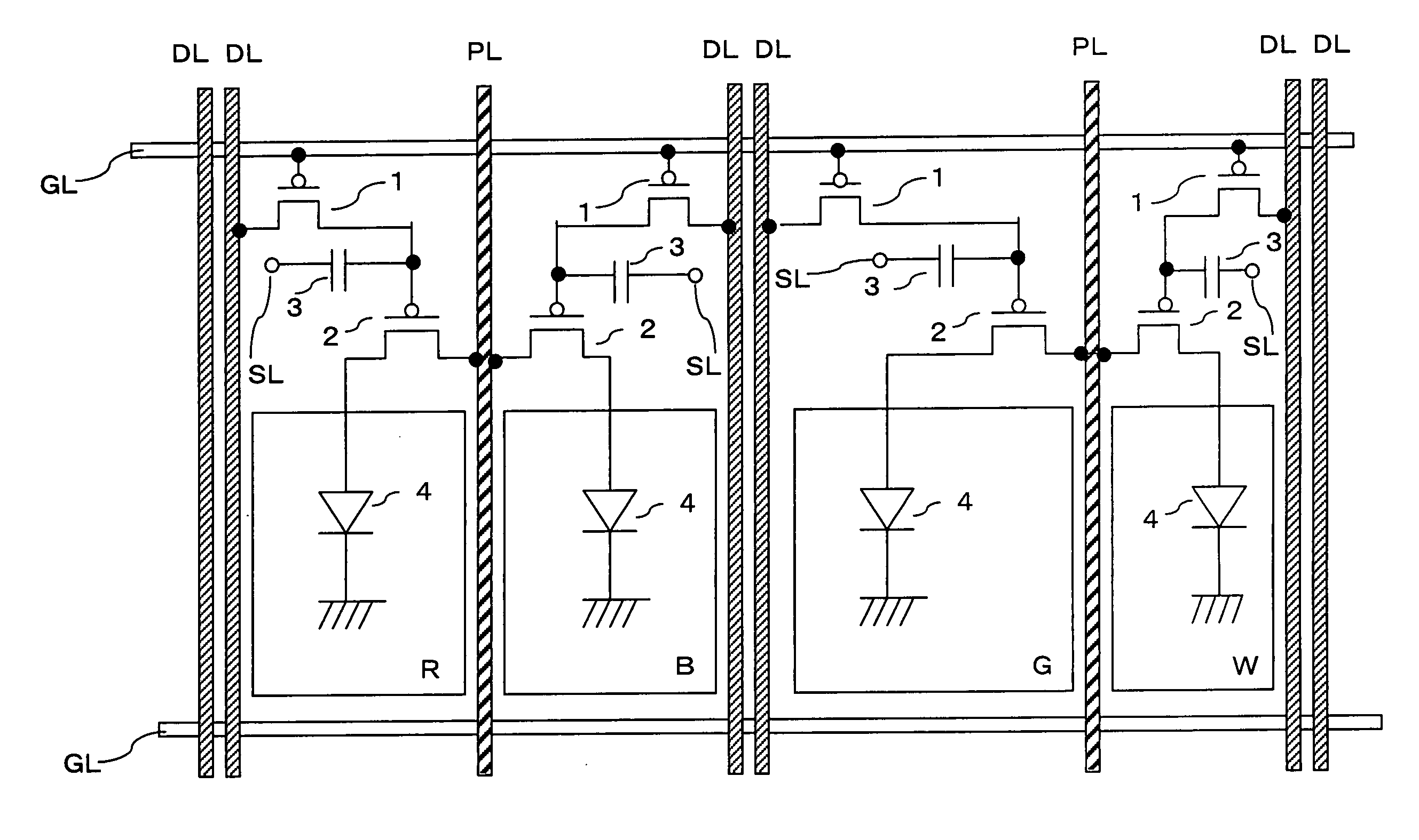
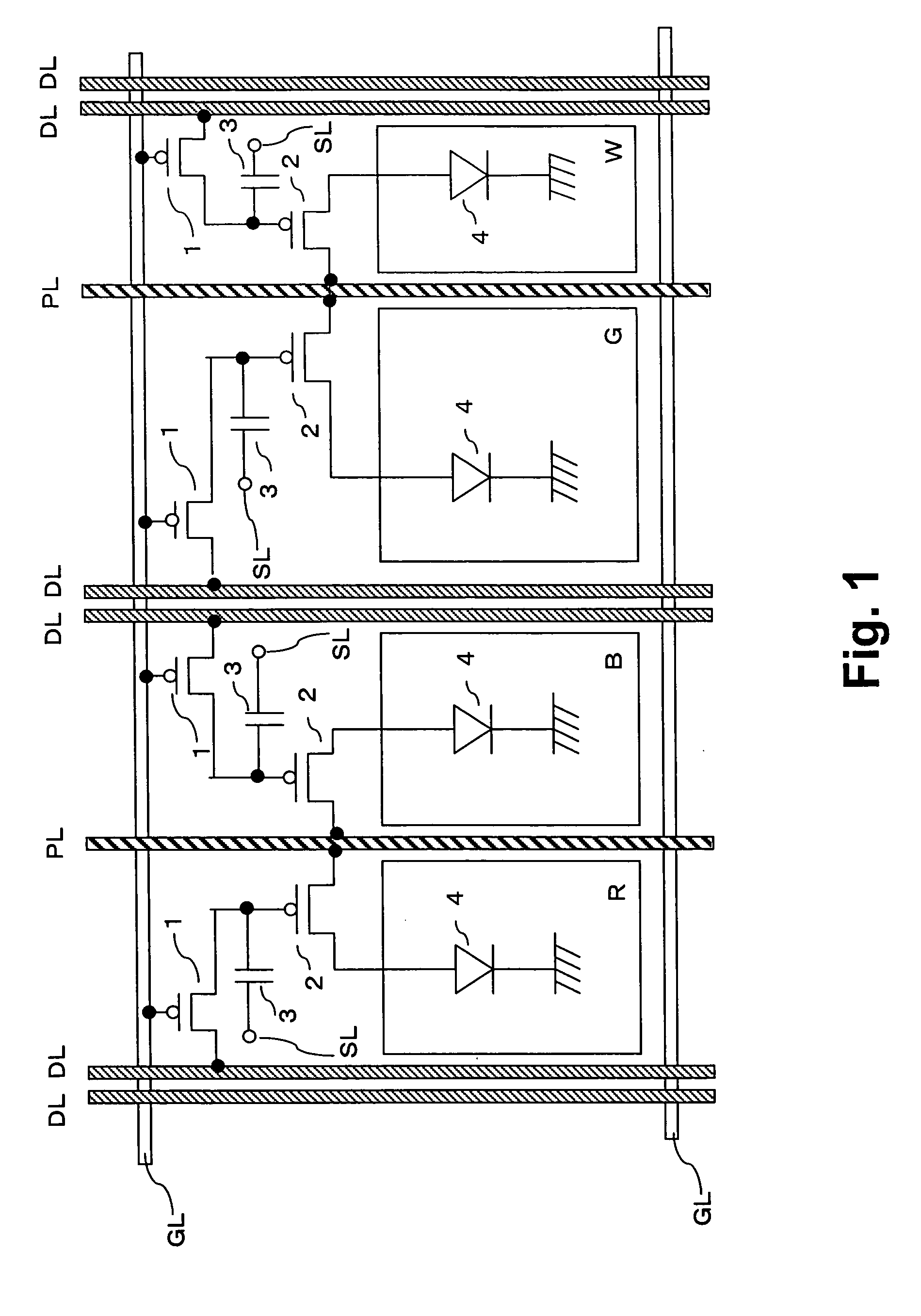
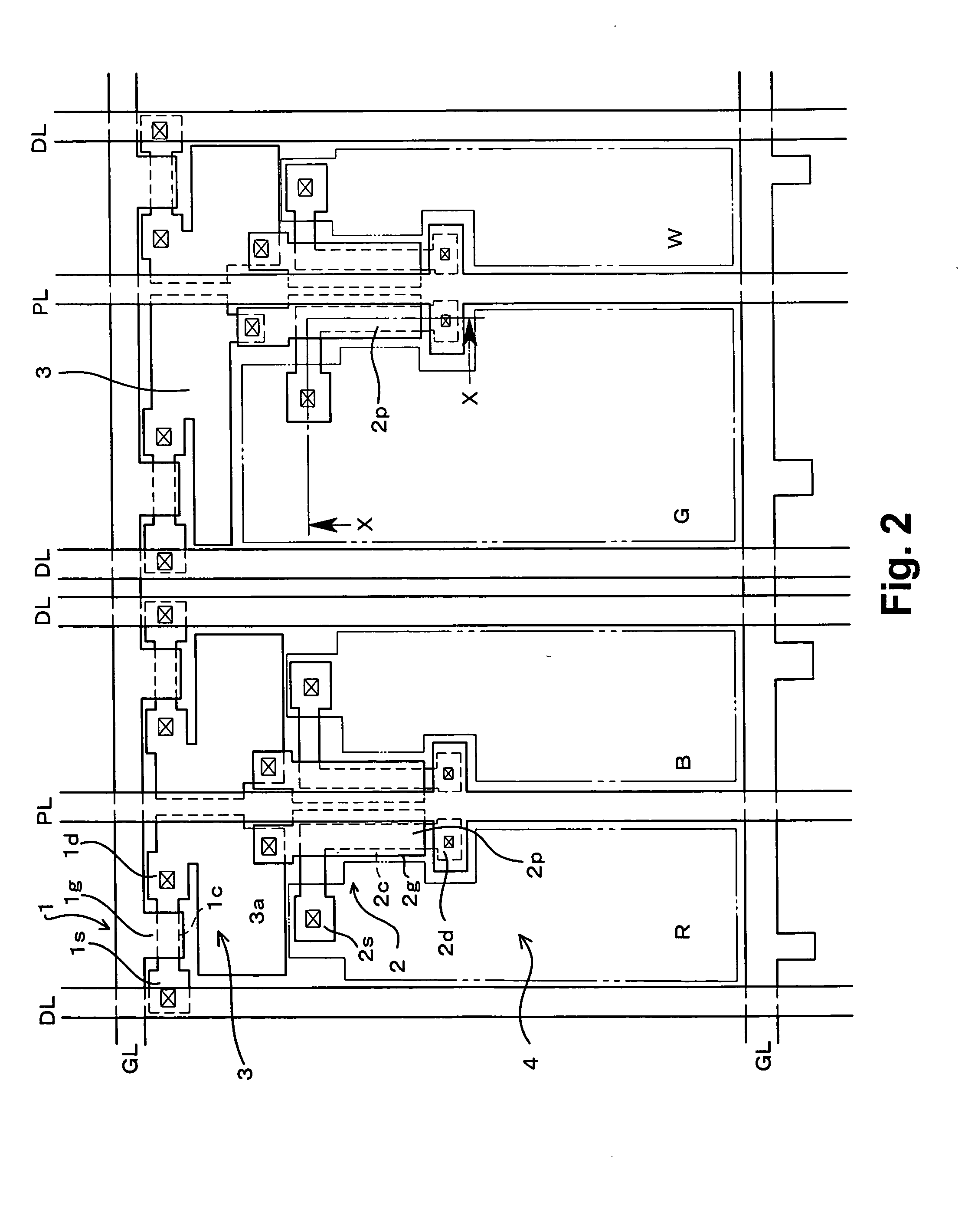
[0016]FIG. 1 schematically shows a structure of an embodiment of the present invention. A single data line DL is provided for each pixel column and mounted such that two data lines DL are placed between pixel columns for every other pixel column. A power supply line PL is placed in a space between pixel columns, where a data line DL is not mounted. A gate line GL is mounted between pixel rows.

[0017] In each pixel, a selection TFT 1, a driver TFT 2, a holding capacitor 3, and an organic EL element 4 are provided. In this example, the selection TFT 1 is a p-channel TFT, and connected, via its source, to a data line DL, via its drain, to the gate of the driver TFF 2, and via its gate, to a gate line GL.

[0018] The driver TFT 2 is also a p-channel TFT, and connected, via its source, to a power supply line PL, and via its drain, to the node of the organic EL elem...


PUM


Abstract

A drive transistor is connected, via its drain region, to a power supply line, and, via its source region, to a transparent electrode of an organic EL element. The channel region is formed bent into a substantially L shape. This arrangement is able to simplify the arrangement of a gate electrode by providing the gate electrode so as to run straight over a channel region in parallel to the power source line. Accordingly, the aperture ratio is increased.

Description

CROSS-REFERENCE TO RELATED APPLICATIONS [0001] The entire disclosure of Japanese Patent Application No. 2003-337933 including specification, claims, drawings and abstract is incorporated herein by reference. BACKGROUND OF THE INVENTION [0002] 1. Field of the Invention [0003] The present invention relates to an organic electroluminescence panel where organic EL elements, each having at least an organic light emitting layer between a pair of electrodes, are arranged in matrix. [0004] 2. Description of the Related Art [0005] Organic electroluminescence (hereinafter referred to as EL) panels have been receiving attention as one of the next generation flat displays to take place the liquid crystal displays. In the display panels (hereinafter referred to as an organic EL panel), the color of light emitted by each pixel can be determined depending on the kind of light emitting material used to form an organic light emitting layer for the pixel. Thus, pixels for different color light are fo...

Claims


Application Information

Patent Timeline
IPC IPC(8): H01L51/50G09F9/30G09G3/10H01L21/77H01L27/12H01L27/32H01L29/786H05B33/00H05B33/12H05B33/14H05B44/00
CPCG09G2300/0452G09G2300/0842H01L27/1214H01L29/78696H01L27/3244H01L27/3262H01L27/3213H10K59/351H10K59/12H10K59/1213H01L27/12
Inventor MATSUMOTO, SHOICHIRO
Owner SANYO ELECTRIC CO LTD
Why Eureka
Try Eureka