Resistive device and method for its production

a resistive device and resistive technology, applied in the direction of solid-state devices, semiconductor devices, basic electric elements, etc., can solve the problems of reducing achieve the effect of effective change of the electric resistance of the resistive device, increase the resistance-determining width of the current path, and wide resistance value rang

Active Publication Date: 2005-04-14
INFINEON TECH AG
View PDF13 Cites 0 Cited by
  • Summary
  • Abstract
  • Description
  • Claims
  • Application Information

AI Technical Summary

Benefits of technology

[0017] One advantage of the present invention is that by influencing the resistance-determining width of a current path through the more highly doped first region, a particularly effective change of the electric resistance of the resistive device is possible. The present invention thus allows a change of the electric resistance of the resistive device within a wide resistance value range. Thus, also with a wide spread of the original resistance values of resistive devices effected with simple and inexpensive technological means, a setting, or an adjustment, to a predetermined resistance value may be performed.
[0018] In accordance with a preferred embodiment, the second region having the lower dopant concentration is convex or, in particular, wedge-shaped at the portion of the doping boundary determining the resistance-determining width of the current path. Particularly a wedge-shaped second region or particularly a second region wedge-shaped at the portion of the doping boundary determining the resistance-determining width of the current path has the advantage that even a small shift of the doping boundary between the first region and the second region results in a significantly greater increase in the resistance-determining width of the current path through the first region.
[0019] In accordance with an embodiment, the first region is simply contiguous and the second region contiguous. Preferably, the second region extends primarily transverse to the basic current flow direction of the resistive device between the terminals thereof, wherein the resistance-determining width of the current path through the first region is equal to the total width of the resistive region minus the expansion of the second region.
[0020] In an alternative embodiment, the first region is multiply contiguous and the second region is non-contiguous. The second region consists of several contiguous sub-regions that are arranged substantially one after the other or, preferably, substantially next to one another in the direction of the basic current flow direction of the resistive device. Every single sub-region is, in turn, preferably implemented such that a shift of the doping boundary by a shift distance results in an increase in the resistance-determining width of the current path through the first region, that is larger than the shift distance.
[0021] The present invention is implementable both as a resistive device and a method for producing a resistive device.
[0022] Preferred further developments of the present invention are defined in the dependent claims.

Problems solved by technology

This results in an increase in the resistance-determining width of the current path through the first region and thus a reduction of the electric resistance of the resistive device.

Method used


Image

  • Resistive device and method for its production
  • Resistive device and method for its production
  • Resistive device and method for its production

Examples


Embodiment Construction

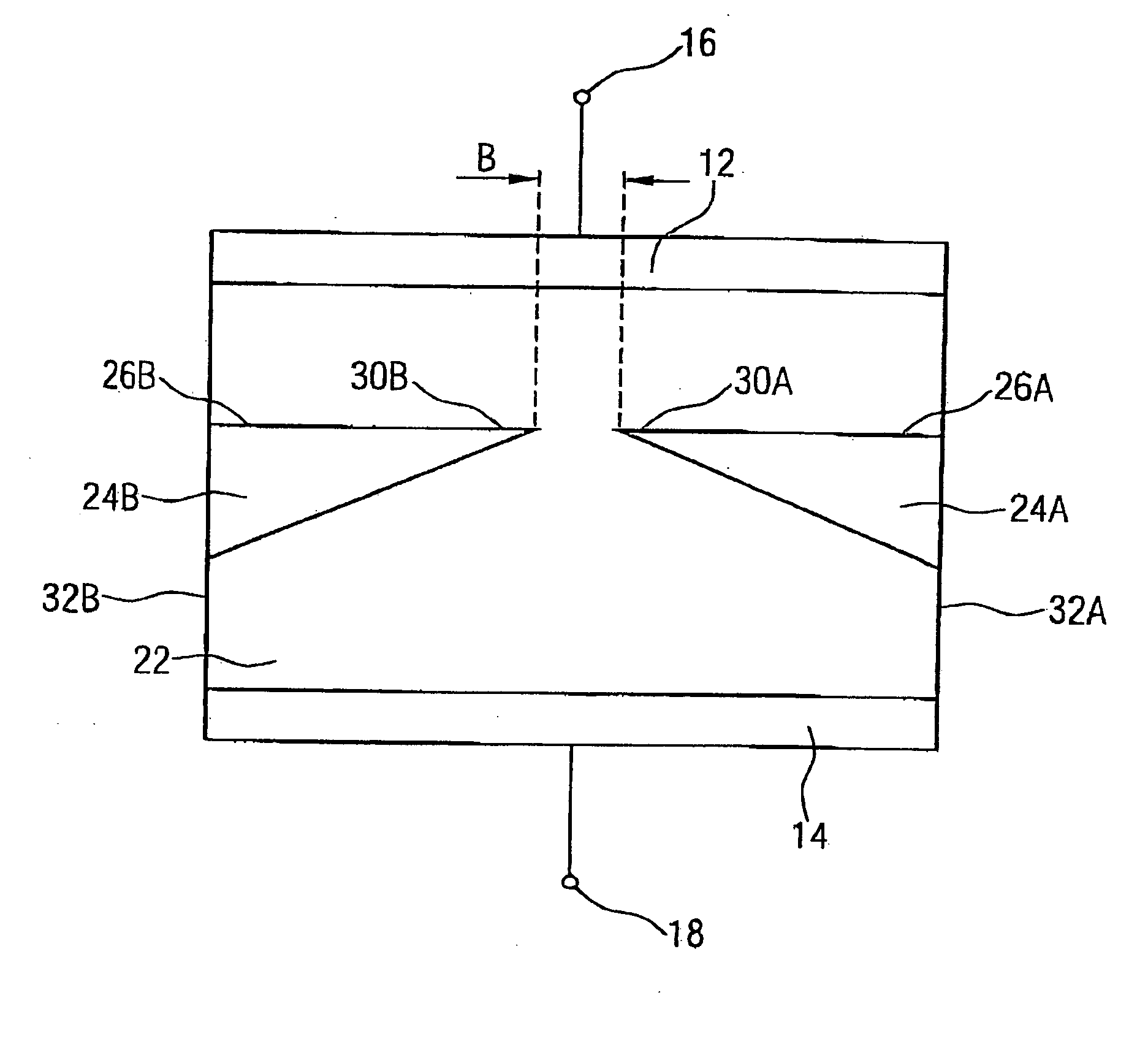
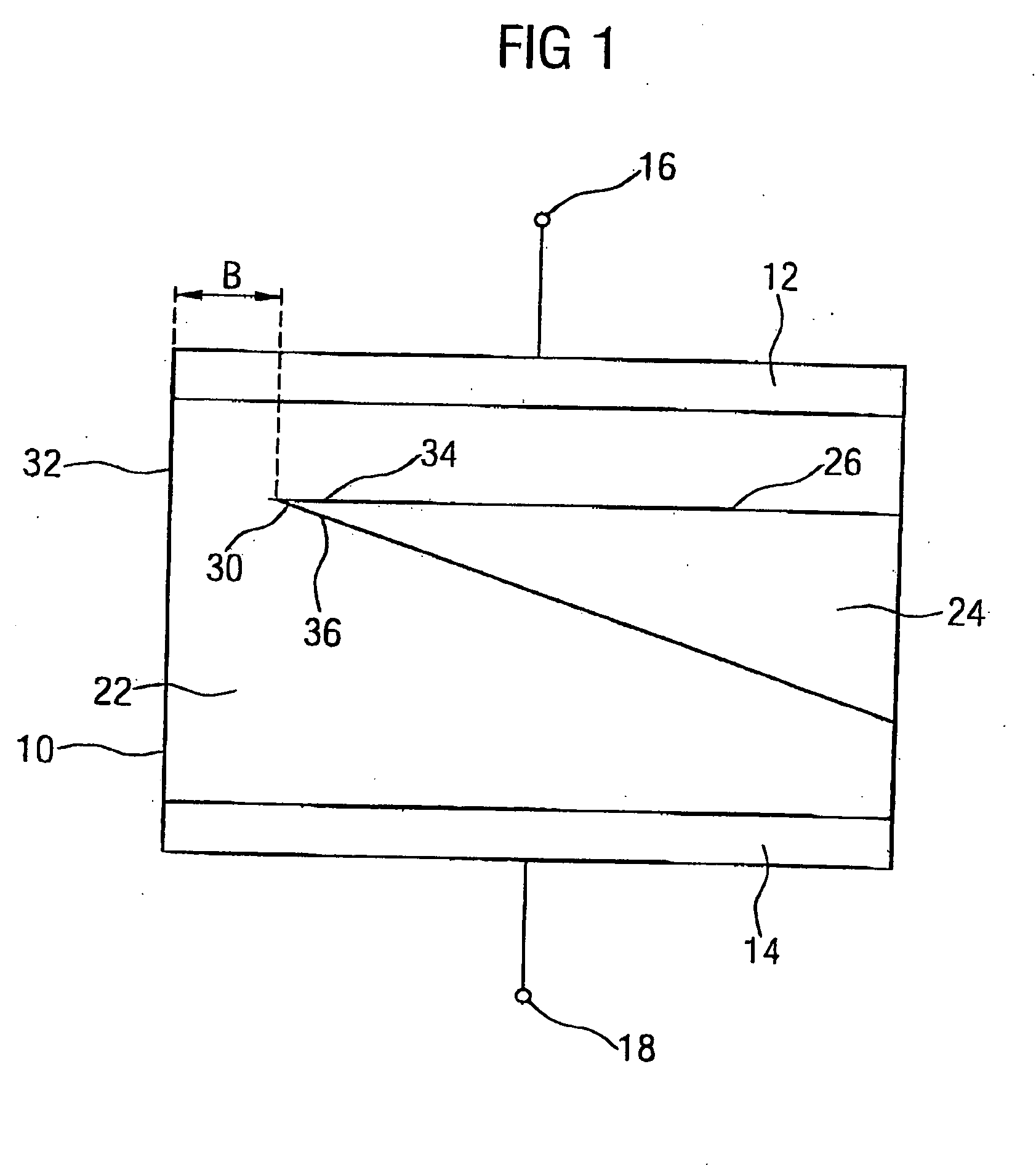
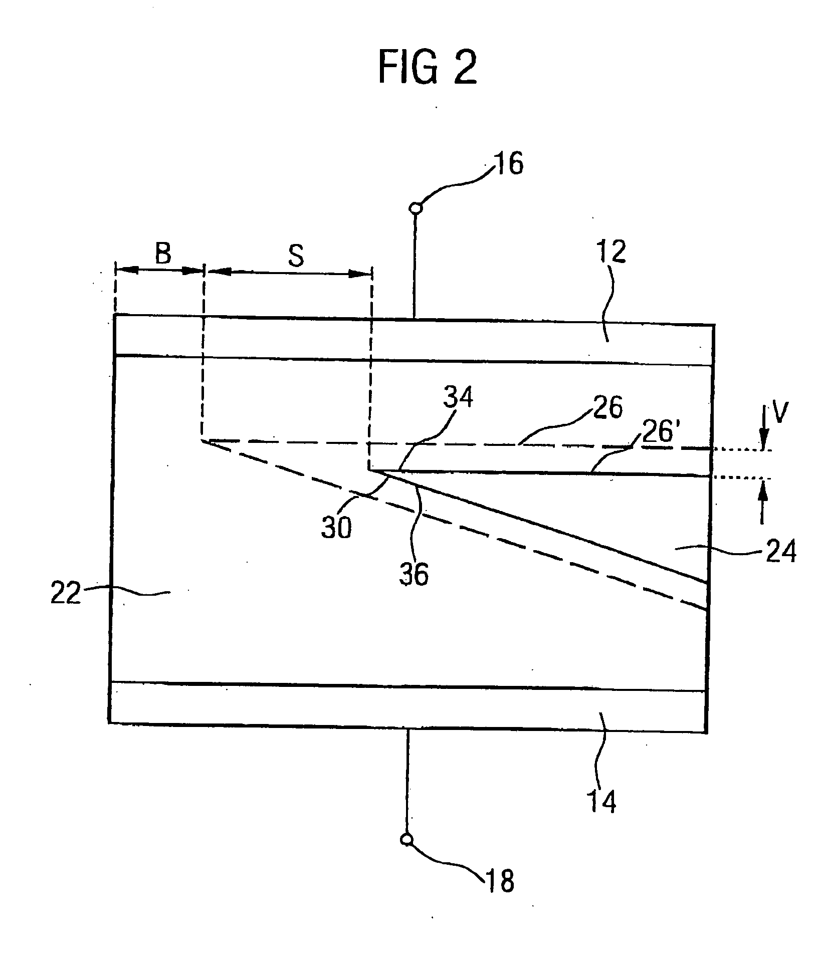
[0028] FIG. is a schematic top-view of a resistive device according to a first embodiment of the present invention. The resistive device includes a substantially rectangular resistive region of a semiconductor material that has been deposited preferably amorphously or polycrystallinely on a preferably diffusion-inhibiting insulating layer, preferably a semiconductor oxide layer. A crystalline layer mounted on a preferably diffusion-inhibiting insulating layer corresponding to the SOI technology is also employable. Highly doped contact strips 12, 14 are provided along two parallel sides of the resistive region 10 opposing each other. The resistive region 10 is connected electrically conducting with terminals 16, 18 via the highly doped contact strips 12, 14 and, if applicable, resistive contacts. The arrangement of the contact strips 12, 14 and the terminals 16, 18 determines a basic current flow direction in the resistive region 10.

[0029] The resistive region 10 includes a first re...


PUM


Abstract

A resistive device includes a resistive region of a semiconductor material that includes a first region and a second region, wherein the first region has a higher dopant concentration than the second region, and wherein a resistance-determining width of a current path through the first region is determined by a portion of a doping boundary between the first region and the second region.

Description

CROSS-REFERENCE TO RELATED APPLICATION [0001] This application claims priority from German Patent Application No. 10338689.0, which was filed on Aug. 22, 2003, and is incorporated herein by reference in its entirety. BACKGROUND OF THE INVENTION [0002] 1. Field of the Invention [0003] The present invention relates to a resistive device whose electric resistance is adjustable as well as a method for its production. [0004] 2. Description of the Related Art [0005] For numerous applications, resistive devices with a defined electric resistance must be produced in integrated circuits. There are several methods for the production of integrated resistive devices, which are, however, generally characterized either by a wide spread of the resistance values or by considerable processing requirements. In order to obtain a defined resistance value, resistive devices are often adjusted, or set, afterwards. Conventionally, however, this adjustment is only possible within a relatively small range. ...

Claims


Application Information

Patent Timeline
Patent Type & Authority Applications(United States)
IPC IPC(8): H01L21/02H01L27/08
CPCH01L27/0802Y10S257/904H01L28/20
Inventor POMPL, STEFAN
Owner INFINEON TECH AG
Why Eureka
Try Eureka