Electroluminescent display device

Active Publication Date: 2005-04-14
SAMSUNG DISPLAY CO LTD
View PDF5 Cites 52 Cited by
  • Summary
  • Abstract
  • Description
  • Claims
  • Application Information

AI Technical Summary

Benefits of technology

[0015] Therefore, In view of the prior art problems, an object of the present invention is to provide

Problems solved by technology

Further, there is a problem with the organic EL device in that, because the refractive index of the luminous body affects the device, light at an exit angle larger than a critical angle causes total reflection and accordingly cannot be emitted to the exterior.
Otherwise, such fatal degradation may be caused in the organic EL device.
However, the methods listed herein is usable for a large sized substrate, while it has a problem that, in a high definition display configured to have a very small pixel area, it is difficult to manufacture lens having a light focusing capability or to form a reflecting surface that is a side surface.
And, in an organic EL device comprising an emitting layer with a thickness of several microns or less, it is very difficult to form a reflecting mirror on a side surface of the device even with a super fine processing technique, and the reflecting mirror may be formed but manufacturing cost significantly increases, which greatly obstructs a practical use.
However, it is considered that forward light-emitting efficiency in this method may be enhanced but cannot prevent total reflection.
That is, there is a problem w

Method used


Image

  • Electroluminescent display device
  • Electroluminescent display device
  • Electroluminescent display device

Examples


Example

COMPARATIVE EXAMPLE 1

[0099] A sequence of fabricating an organic thin film electroluminescent device used in Comparative example 1 is shown. FIG. 8 is a structure view of Comparative example 1.

[0100] In FIG. 8, the device was configured by stacking a glass substrate 31, an anode (ITO) 32, a hole injecting layer (α-NMP) 33, an emitting layer (AlQ) 34, and a cathode (MgAg) 35 in this order.

[0101] An indium tin oxide alloy (ITO) was formed on the glass substrate 31 of 50 mm×25 mm (NA45 produced by HOYA, 1.1 mm thick) by a sputtering method, and was used as the anode 32. The film thickness of the ITO was 100 nm, and sheet resistance was 20Ω / □. And, the formed ITO was patterned using a metal mask to be a stripe of 2 mm×50 mm.

[0102] Subsequently, the hole injecting layer 33, the emitting layer 34 and the cathode 35 were each stacked in this order on the ITO layer of the anode 32. Further, the organic layers (the hole injecting layer 33 and the emitting layer 34) and the cathode 35 wer...

Example

COMPARATIVE EXAMPLE 2

[0104] An organic EL device was fabricated by sequentially stacking an anode, a hole injecting layer, an emitting layer, and a cathode on a quartz glass (1.1 mm thick). Further, processes following the anode formation process were carried out in the same condition as Comparative example 1.

Example

COMPARATIVE EXAMPLE 3

[0105] Comparative example 3 is the same as Embodiment 1 except that only the intermediate layer was eliminated from the structure and fabricating process.


PUM

PropertyMeasurementUnit
Thicknessaaaaaaaaaa
Thicknessaaaaaaaaaa
Thicknessaaaaaaaaaa

Abstract

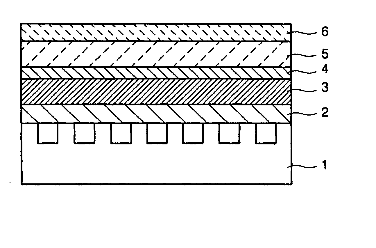
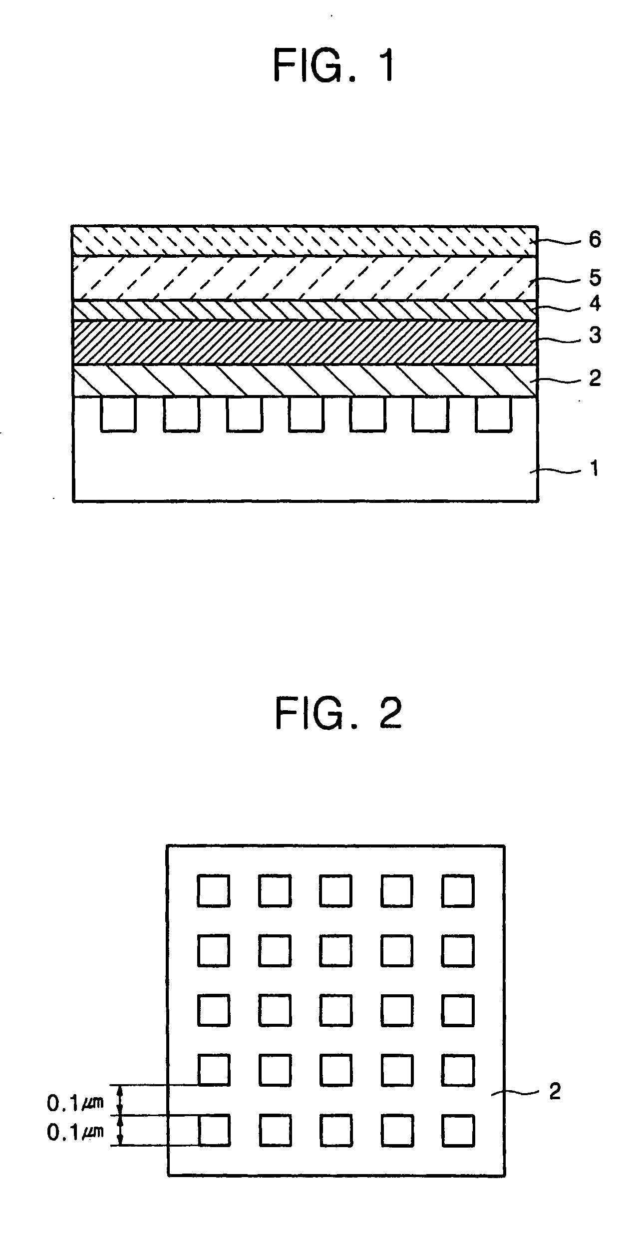
The present invention relates to an organic electroluminescent device. There is provided an organic electroluminescent device with a good luminescence property and high luminous efficiency in which the organic electroluminescent device has a diffraction grating 2 on the surface of the substrate 1 and an organic EL layer 5 including an emission layer between an anode 4 an a cathode 6 via an intermediate layer 3.

Description

CROSS-REFERENCE TO RELATED APPLICATION [0001] This application claims the benefit of Japanese Patent Application No. 2003-144769, filed May 22, 2003, the disclosure of which is hereby incorporated herein by reference in its entirety. BACKGROUND OF THE INVENTION [0002] 1. Field of the Invention [0003] The present invention relates to an organic electroluminescent device having a good luminescent state and excellent luminous efficiency. [0004] 2. Description of the Related Art [0005] The organic electroluminescent device (hereinafter, organic EL device) is an emissive device using a principle in which a fluorescent material emits light using recombination energy of holes injected from an anode and electrons injected from a cathode by electric field application. A representative example of a study on this organic EL device includes a low voltage driving organic EL device using a stacked device, which has been reported by C. W. Tang et al (e.g., see C. W. Tang, S. A. VanSlyke, Applied P...

Claims


Application Information

Patent Timeline
IPC IPC(8): H01L51/50H05B33/02H01L51/52H05B33/22
CPCH01L51/5262H01L51/5275H01L51/5268H10K50/85H10K50/854H10K50/858H05B33/22
Inventor ONISHI, YASUHARUTOGUCHI, SATORUYAMANARI, JUNICHIISHIKAWA, HITOSHIGOTOH, TOMOHISAKAMIJO, ATSUSHI
Owner SAMSUNG DISPLAY CO LTD
Why Eureka
Try Eureka