

Transfer substrate and method of manufacturing a display apparatus
- Summary
- Abstract
- Description
- Claims
- Application Information
AI Technical Summary
Benefits of technology
Problems solved by technology
Method used
Image

Examples
examples
[0101]With regard to the formation of the light emitting layers, in which the thermal transfer is applied, an OLED that emits green light and an OLED that emits red light were produced while changing the host material and the luminescent dopant material as follows. A current efficiency and a half-life of luminance of each of the obtained OLEDs were measured, and comparison values obtained by comparing the above OLEDs and OLEDs in which light emitting layers are formed by vapor deposition were calculated.
examples 1 to 16
See Table 1 Below
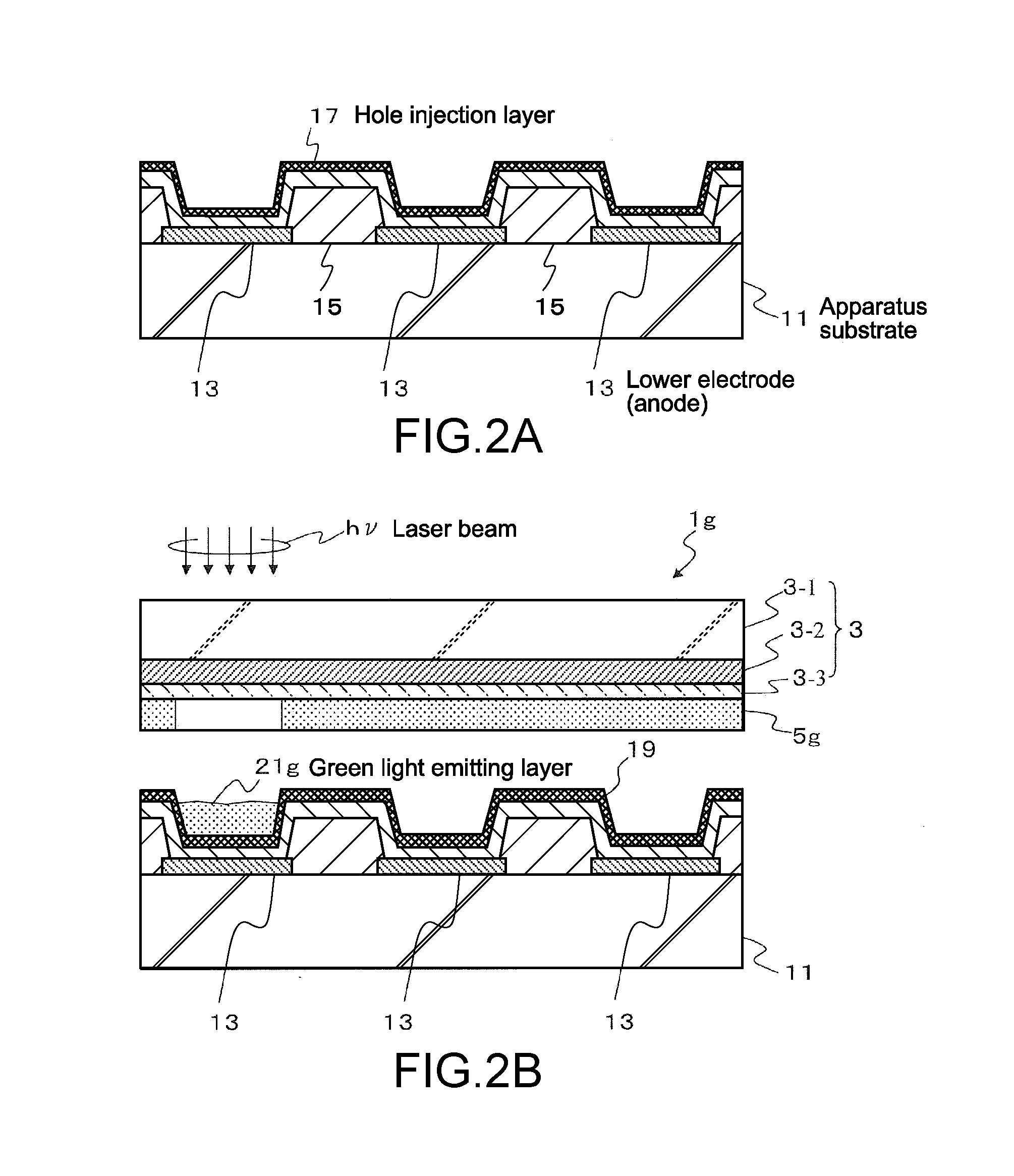
[0102]A thermal transfer using laser irradiation as a heat source was applied and the OLED that emits green light was produced as follows.
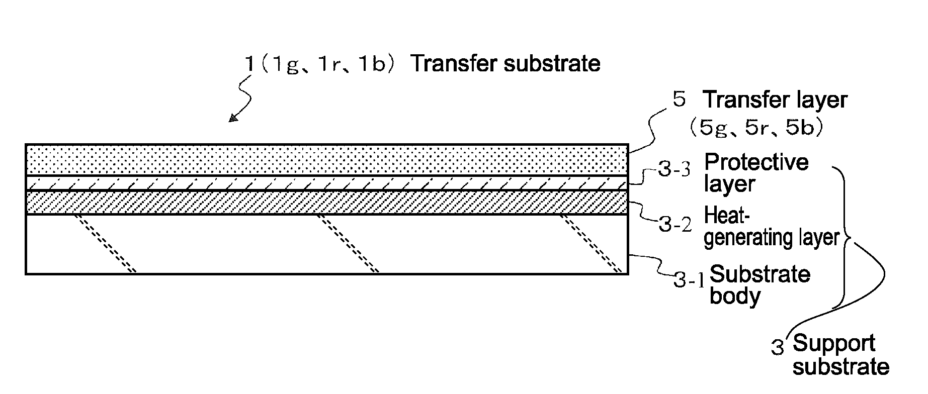
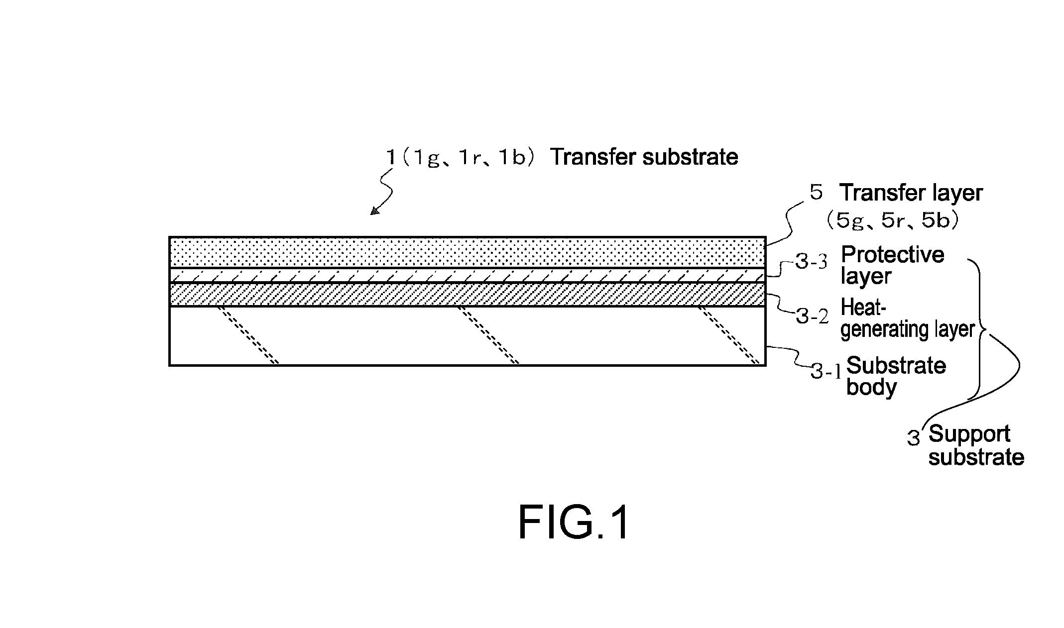
[0103](1) Production of Transfer Substrate
[0104]An anti-reflective layer made of silicon with a thickness of 40 nm and a photothermal conversion layer made of molybdenum (Mo) with a thickness of 200 nm were sequentially formed on a glass substrate having a thickness of 1 mm (substrate body 3-1) by a normal sputtering method, to thereby form a heat-generating layer 3-2 having a laminated structure. Next, a protective layer 3-3 made of silicon nitride (SiNx) was formed on the photothermal conversion layer (heat-generating layer 3-2) in a thickness of 50 nm by CVD. Then, a green transfer layer 5g in which a host material was mixed with 5 wt % of a guest material of green luminance was formed on the protective layer 3-3 in a thickness of 30 nm by vapor deposition, thus obtaining a transfer substrate 1g. The host materials and the gues...
examples 17 to 32
See Table 2 Below
[0111]A thermal transfer using heating with a heater as a heat source was applied and the OLED that emits green light was produced. Processes in Examples 17 to 32 were the same as those performed in Examples 1 to 16 except that the thermal transfer due to heating with a heater was performed in the process (3) in Examples 1 to 16. In the thermal transfer, a temperature of heating due to the heater was set to a lowest temperature at which the transfer could be performed (290° C.), and a temperature of the apparatus substrate was controlled to be 20° C. by cooling water in order to prevent the heat from being transmitted to the apparatus substrate. It should be noted that the host materials and the guest materials of green luminance that constitute the light emitting layer are shown in Table 2 below.
PUM
| Property | Measurement | Unit |
|---|---|---|
| Temperature | aaaaa | aaaaa |
| Temperature | aaaaa | aaaaa |
| Temperature | aaaaa | aaaaa |
Abstract
Description
Claims
Application Information