Methods and apparatus for testing continuity of electrical paths through connectors of circuit assemblies

a technology of circuit assembly and connector, which is applied in the direction of cathode-ray oscilloscope, instruments, measurement devices, etc., can solve the problems of lack of capacitive coupling between the ic lead frame and the tester's sense plate, the defect is “open”, and interferes with the success of capacitive lead-frame testing

Inactive Publication Date: 2005-04-14
AGILENT TECH INC
View PDF10 Cites 24 Cited by
  • Summary
  • Abstract
  • Description
  • Claims
  • Application Information

AI Technical Summary

Problems solved by technology

Note, however, that one of the leads 108 is not soldered to the printed circuit board, thereby resulting in an “open” defect.
If CSense is chosen to be significantly larger than any possible CJoint, a bad lead will result in the AC detector seeing a capacitance near CJoint.
Over the years, various factors have interfered with the success of capacitive lead-frame testing.
One factor is a lack of capacitive coupling between an IC lead-frame and a tester's sense plate.
This problem is largely traced to the on-going miniaturization of IC packages and their lead-frames, as well as the imposition of ground shield and heat sinks between lead-frames and the sensor plate (some of which are internal to an IC's package).
However, they can also interfere with capacitive lead-frame testing in that they sometimes make it difficult to position the sense plate of a capacitive lead-frame tester in close enough proximity to their lead-frames.
Another factor that has interfered

Method used


Image

  • Methods and apparatus for testing continuity of electrical paths through connectors of circuit assemblies
  • Methods and apparatus for testing continuity of electrical paths through connectors of circuit assemblies
  • Methods and apparatus for testing continuity of electrical paths through connectors of circuit assemblies

Examples


Embodiment Construction

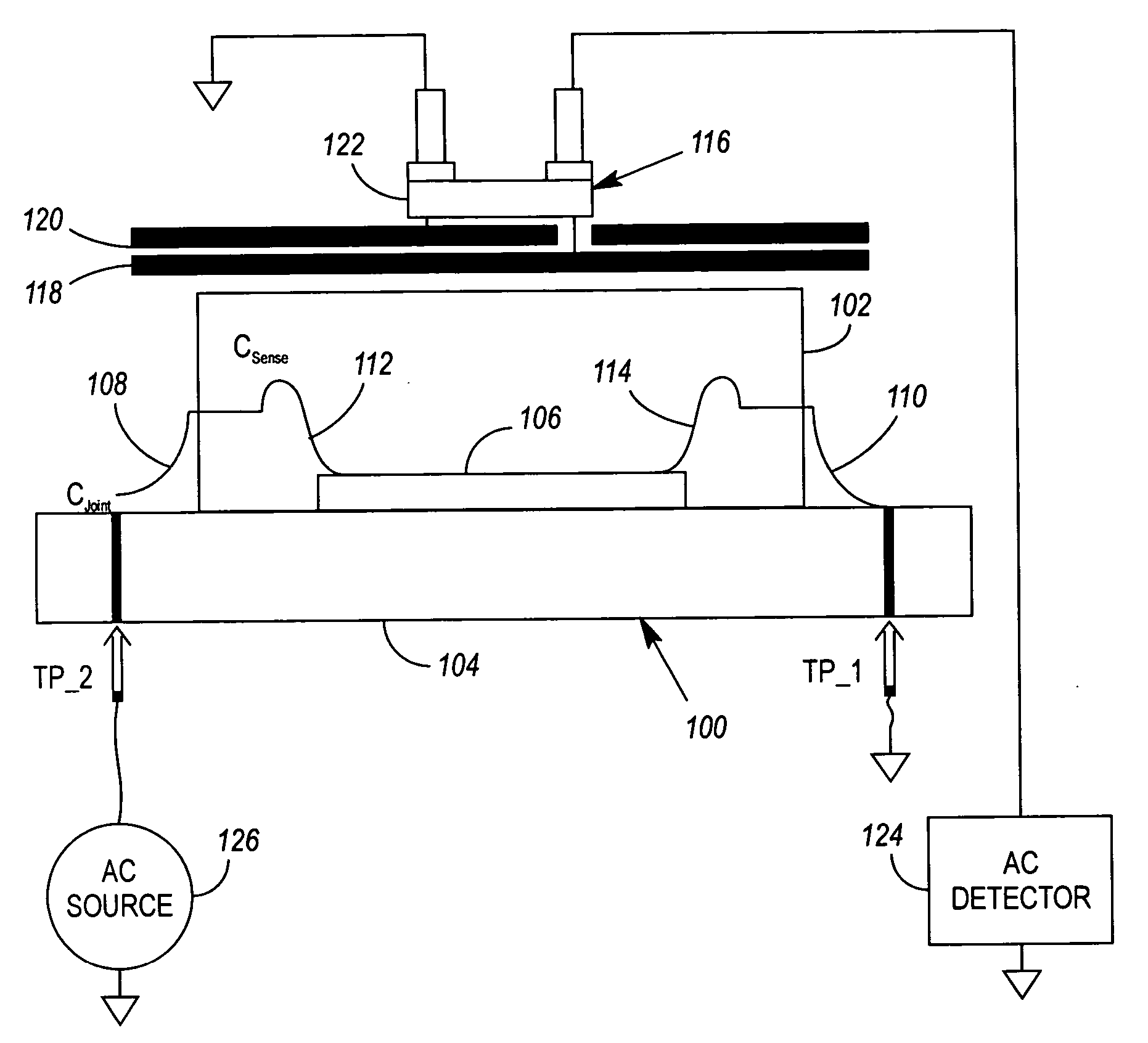
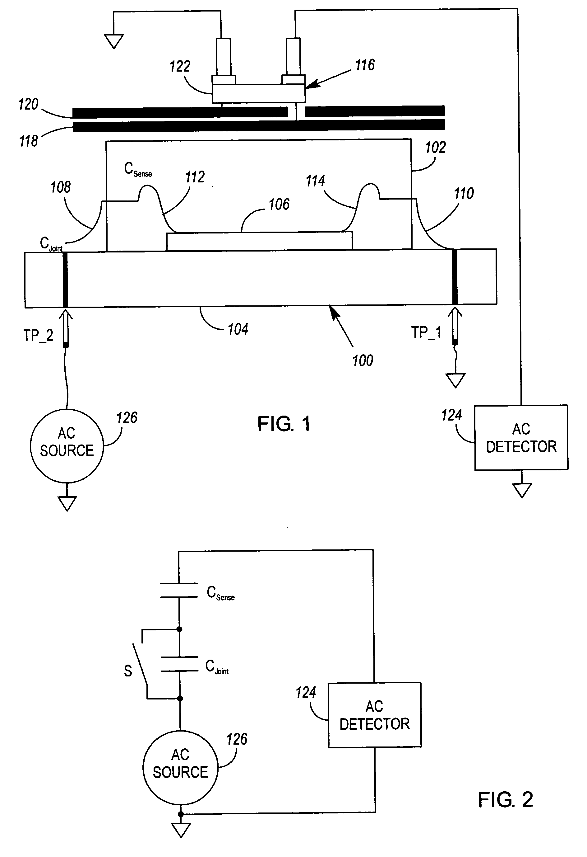
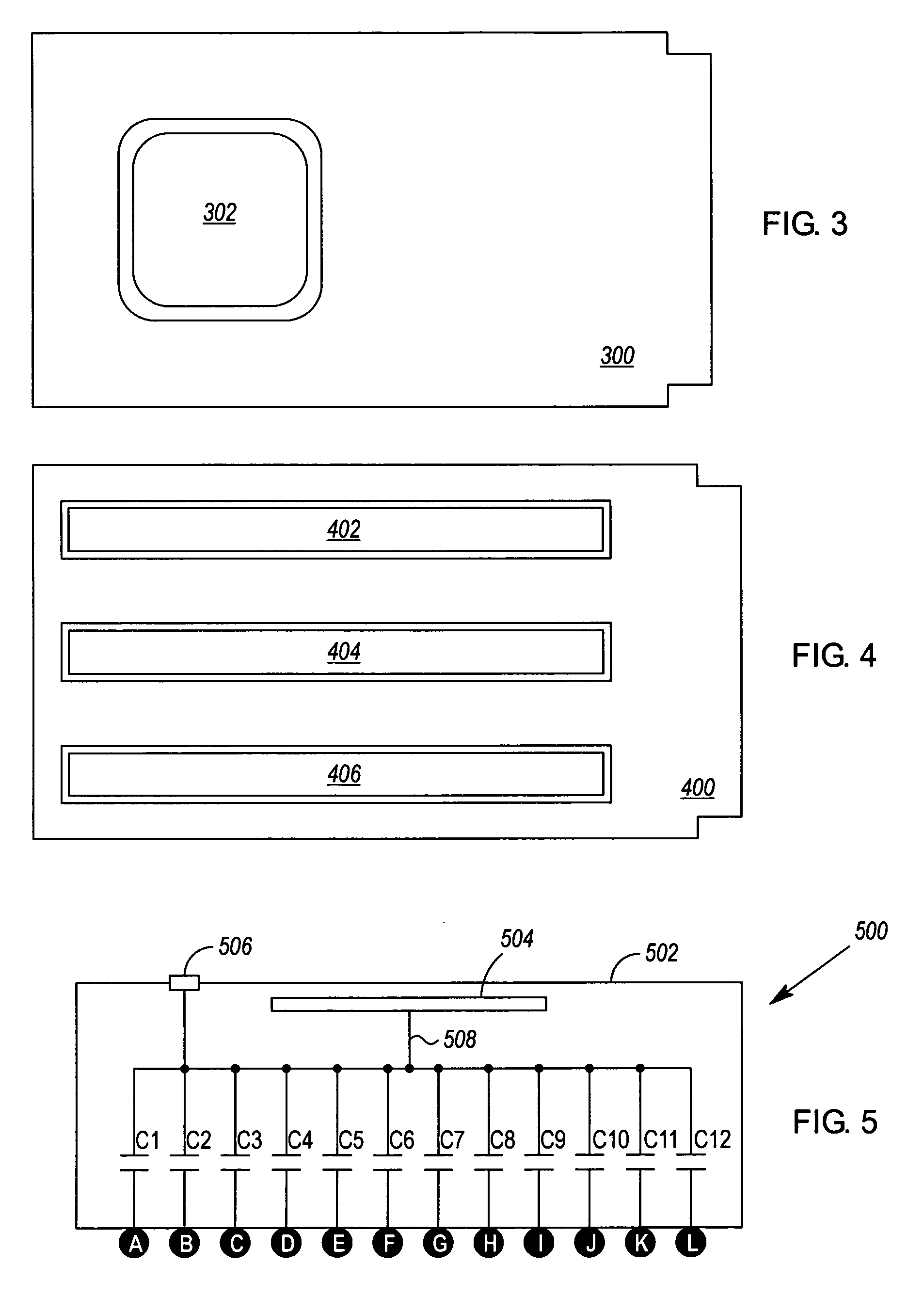
[0026]FIGS. 3 & 4 illustrate circuit assemblies 300, 400 comprising various forms of connectors (e.g., a socket 302 for receiving an integrated circuit (IC) package, and connectors 402, 404, 406 for receiving random access memory (RAM) modules). FIG. 5 illustrates a first exemplary embodiment of a device 500 for testing continuity of electrical paths through a connector of a circuit assembly. By way of example, the device 500 is configured to test the IC socket 302 shown in FIG. 1.

[0027] The device 500 comprises a package 502 containing incomplete or no mission circuitry for the circuit assembly 300 of which the connector under test 302 forms a part. If the device contains no mission circuitry, the device 500 may be produced based on the structural design of the connector 302, and without any knowledge of the functional design of the circuit assembly 300.

[0028] The package 502 is provided with a plurality of contacts (identified as contacts A-L) for mating to a plurality of contac...


PUM


Abstract

A device for testing continuity of electrical paths through a connector of a circuit assembly has a package containing incomplete or no mission circuitry for the circuit assembly. The package is provided with a plurality of contacts for mating to a plurality of contacts of the connector. A test sensor port is integrated with the package. A plurality of passive circuit components are integrated with the package, ones of which are coupled in parallel between ones of the contacts on the package and the test sensor port.

Description

BACKGROUND OF THE INVENTION [0001] During manufacture, circuit assemblies (e.g., printed circuit boards and Multi-Chip Modules) need to be tested for interconnect defects such as open solder joints, broken connectors, and bent or misaligned leads (e.g., pins, balls, or spring contacts). One way to test for such defects is via capacitive lead-frame testing. [0002]FIGS. 1 & 2 illustrate an exemplary setup for capacitive lead-frame testing. FIG. 1 illustrates a circuit assembly 100 comprising an integrated circuit (IC) package 102 and a printed circuit board 104. Enclosed within the IC package is an IC 106. The IC is bonded to the leads 108, 110 of a lead-frame via a plurality of bond wires 112, 114. The leads, in turn, are meant to be soldered to conductive traces on the printed circuit board. Note, however, that one of the leads 108 is not soldered to the printed circuit board, thereby resulting in an “open” defect. [0003] Positioned above the IC package 102 is a capacitive lead-fram...

Claims


Application Information

Patent Timeline
IPC IPC(8): G01R13/02G01R13/28G01R31/02G01R31/04G01R31/26G01R31/28G01R31/312
CPCG01R31/2853G01R31/312G01R31/2896
Inventor PARKER, KENNETH P.BELL, JACOB L.
Owner AGILENT TECH INC
Why Eureka
Try Eureka