Efficient implementation of multiple clock domain accesses to diffused memories in structured ASICs

a structured asic and clock domain technology, applied in the field of very large scale integrated circuit design technology, can solve the problems of less desirable implementation, less die efficiency of less economic value of building structured asics with high port count memories, so as to reduce the availability of diffused memories, maximize memory resources available, and high port count

Inactive Publication Date: 2005-04-14
AVAGO TECH WIRELESS IP SINGAPORE PTE
View PDF2 Cites 4 Cited by
  • Summary
  • Abstract
  • Description
  • Claims
  • Application Information

AI Technical Summary

Benefits of technology

[0008] The objects, features and advantages of the present invention include providing efficient implementation of multiple clock domain accesses to diffused memories in structured ASICs that may (i) allow high port count memories to be implemented on structured ASICs, (ii) maximize memory resources available to a designer and / or (iii) implement multiple clock domains without reducing diffused memory availability.

Problems solved by technology

However, a structured ASIC can provide less design flexibility because much of the IP, particularly memories, is fixed within the base slice of the structured ASIC.
However, high port count memories tend to be less die efficient and are less desirable to implement in a structured ASIC.
Thus, it is economically undesirable to build structured ASICs with high port count memories, yet designers can need such memories.
However, re-architecting the problem to reduce clock domains is not always feasible.
However, the FIFO memory uses another memory block to implement, and again, memory blocks are a finite, limited resource on a structured ASIC.
Thus, the use of the limited memory resource can be somewhat inefficient and can require more routing that can potentially impact performance.
The primary problem is when a designer has to utilize multiple physical memories for FIFOs to implement multiport / clock domain memories, yet also needs most / all the memory blocks for other parts of the design.

Method used


Image

  • Efficient implementation of multiple clock domain accesses to diffused memories in structured ASICs
  • Efficient implementation of multiple clock domain accesses to diffused memories in structured ASICs
  • Efficient implementation of multiple clock domain accesses to diffused memories in structured ASICs

Examples


Embodiment Construction

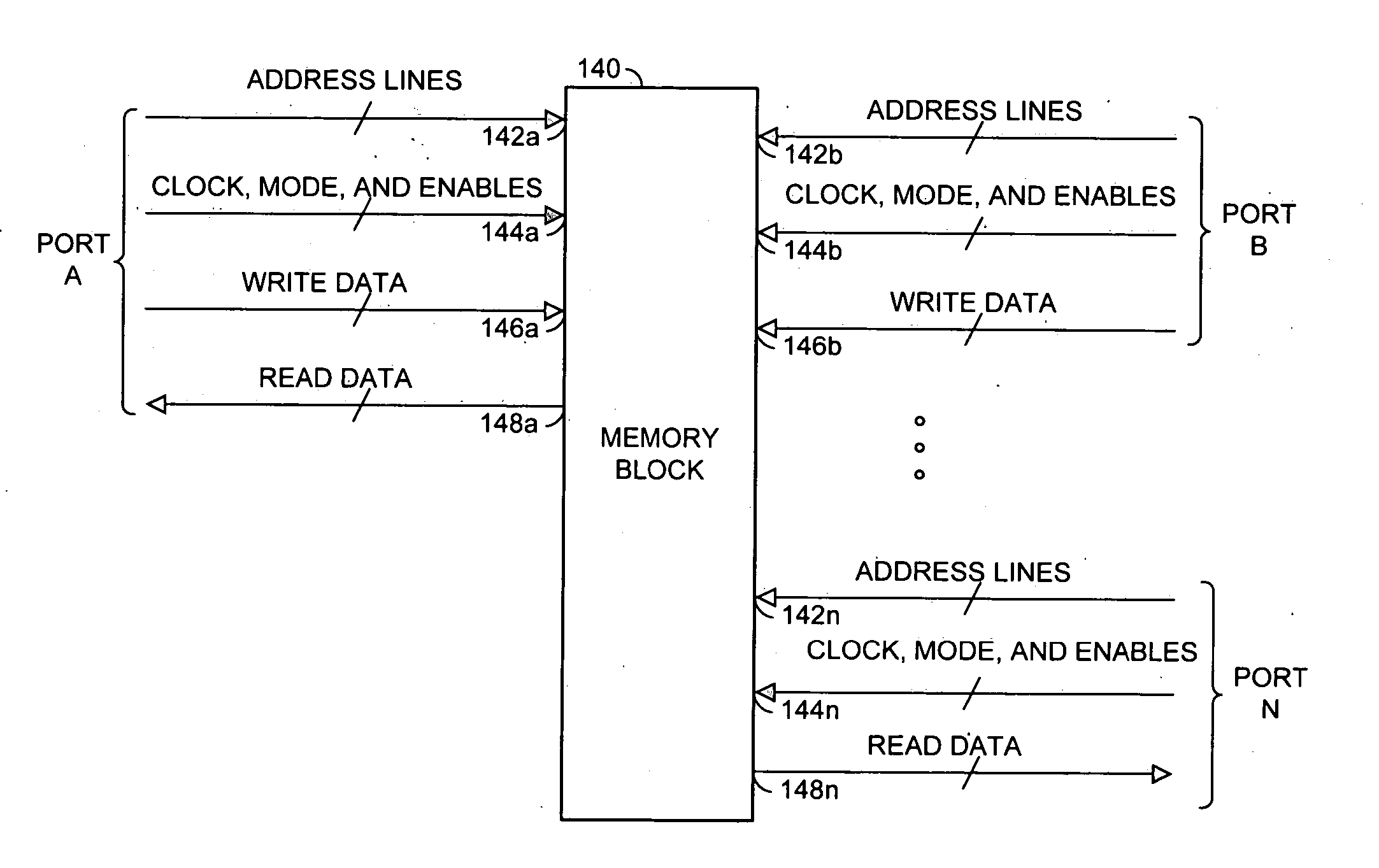
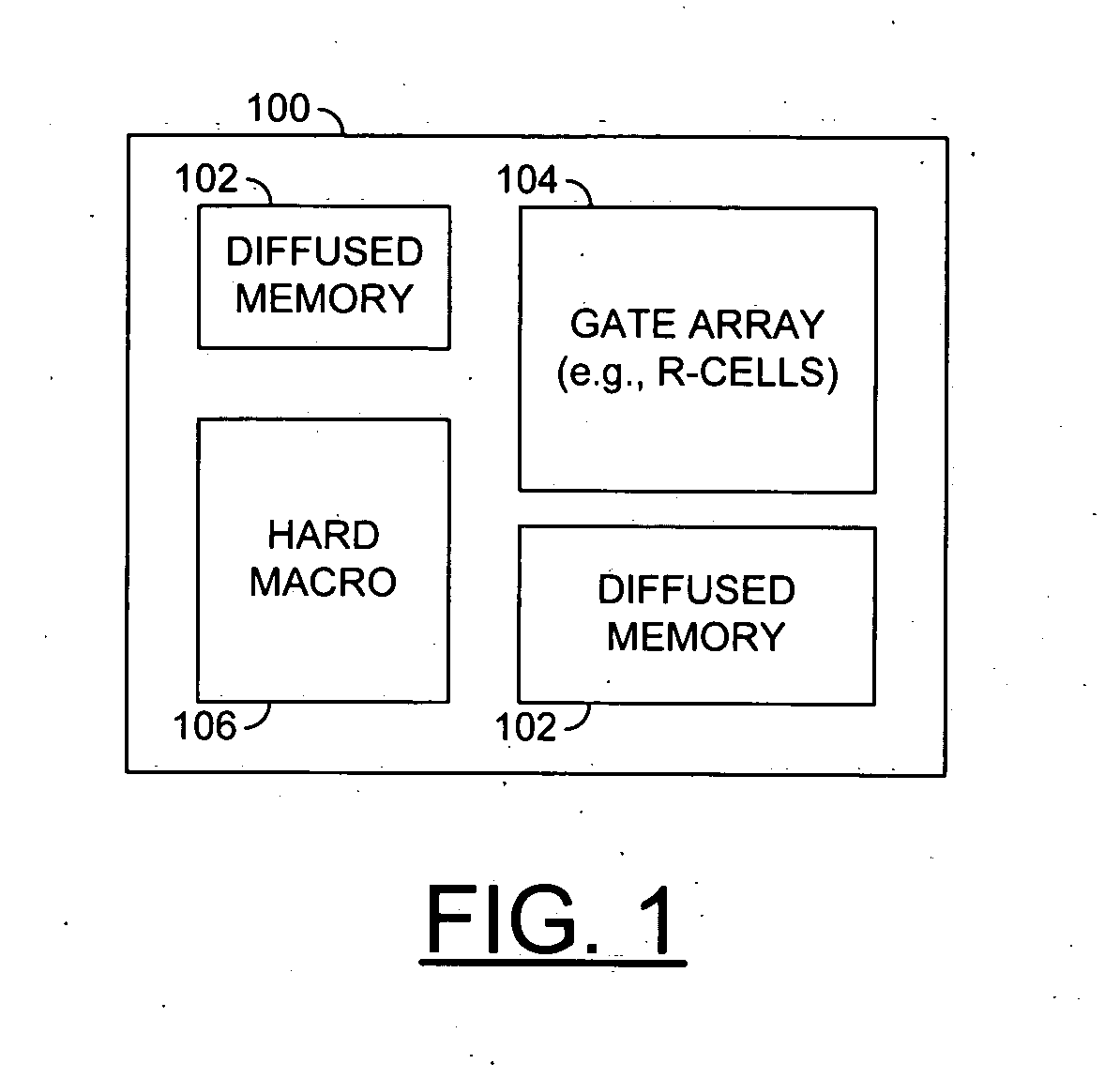
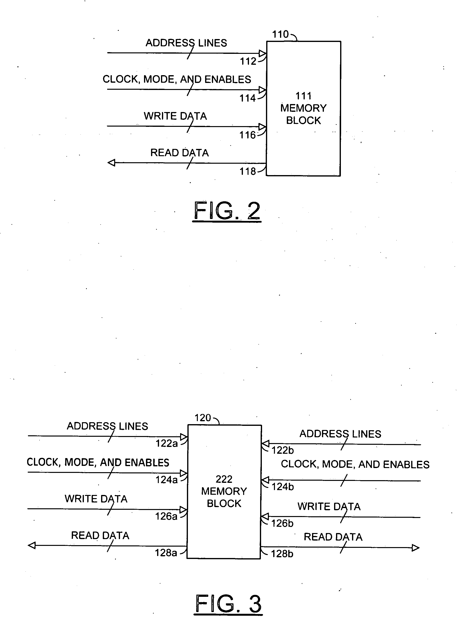
[0020] Referring to FIG. 1, a block diagram of a programmable platform device (or die) 100 is shown in accordance with a preferred embodiment of the present invention. The device 100 may comprise one or more regions of diffused memory 102 and one or more diffused regions 104. The regions 102 and 104 may be distributed around the die 100. The diffused regions 104 may be customized, in one example, as logic and / or memory. For example, the regions 104 may be implemented as a sea-of-gates array. In one example, the regions 104 may be implemented with a number of R-cells. As used herein, R-cells generally refer to an area of silicon designed (or diffused) to contain one or more transistors or gates that have not yet been personalized (or configured) with metal layers. Wire layers may be added to the R-cells to make particular transistors, logic gates and / or storage elements. An R-cell generally comprises one or more diffusions for forming the parts of transistors and / or gates and the con...


PUM


Abstract

A semiconductor device comprising one or more diffused memories and one or more diffused regions. The one or more diffused regions may be configured to provide one or more ports for the one or more diffused memories.

Description

FIELD OF THE INVENTION [0001] The present invention relates to Very Large Scale Integrated (VLSI) circuit design technology generally and, more particularly, to an efficient implementation of multiple clock domain accesses to diffused memories in structured application specific integrated circuits (ASICs). BACKGROUND OF THE INVENTION [0002] Application specific integrated circuits (ASIC) allow a designer to implement exactly the intellectual property blocks (also referred to as IP or macro function blocks) and / or memories needed, in the quantities needed, for a particular design. However, a structured ASIC can provide less design flexibility because much of the IP, particularly memories, is fixed within the base slice of the structured ASIC. Utilizing the fixed memories in ways to satisfy the designer specification, when the memory type is not an exact match has been a focus of product development. Much of the development has focused on joining memories to form different sizes, or s...

Claims


Application Information

Patent Timeline
Patent Type & Authority Applications(United States)
IPC IPC(8): G11C7/22G11C8/04
CPCG11C7/22
Inventor VOGEL, DANNY C.
Owner AVAGO TECH WIRELESS IP SINGAPORE PTE
Why Eureka
Try Eureka