

Image forming apparatus, image forming process, and process cartridge
a technology of image forming and process cartridge, which is applied in the direction of electrographic process apparatus, corona discharge, instruments, etc., can solve the problem of unsatisfactory understanding of the reason, and achieve the effect of reducing the wear of the photoconductor
Active Publication Date: 2005-04-21
RICOH KK
View PDF40 Cites 10 Cited by
- Summary
- Abstract
- Description
- Claims
- Application Information
AI Technical Summary
Benefits of technology
[0032] The object of the present invention to provide an image forming apparatus, an image forming process and a process cartridge, in which the charging hazard is controlled under repeated usage of the photoconductor, the charging uniformity is maintained, the abrasion wear of the photoconductor is reduced, and images may be formed stably even under repeated usage.
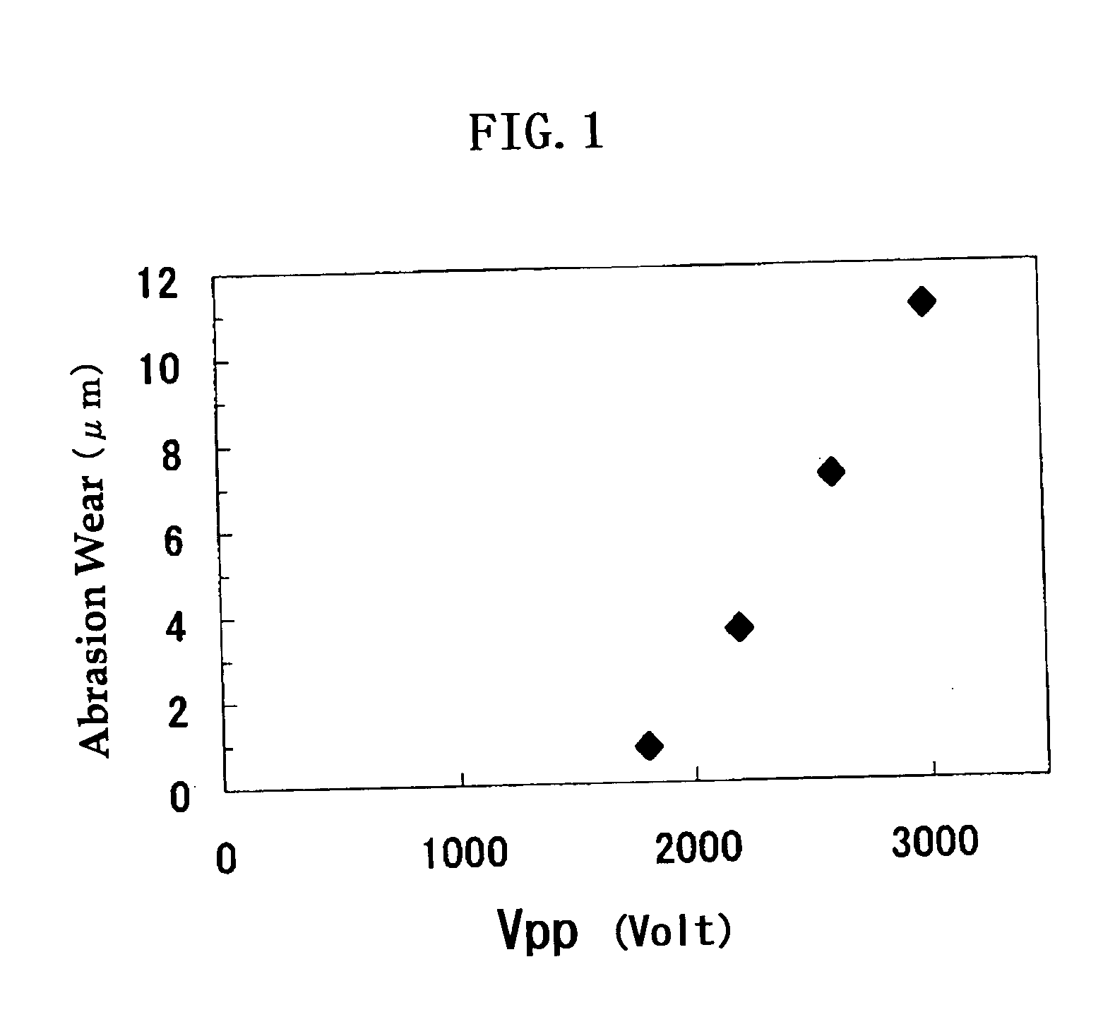
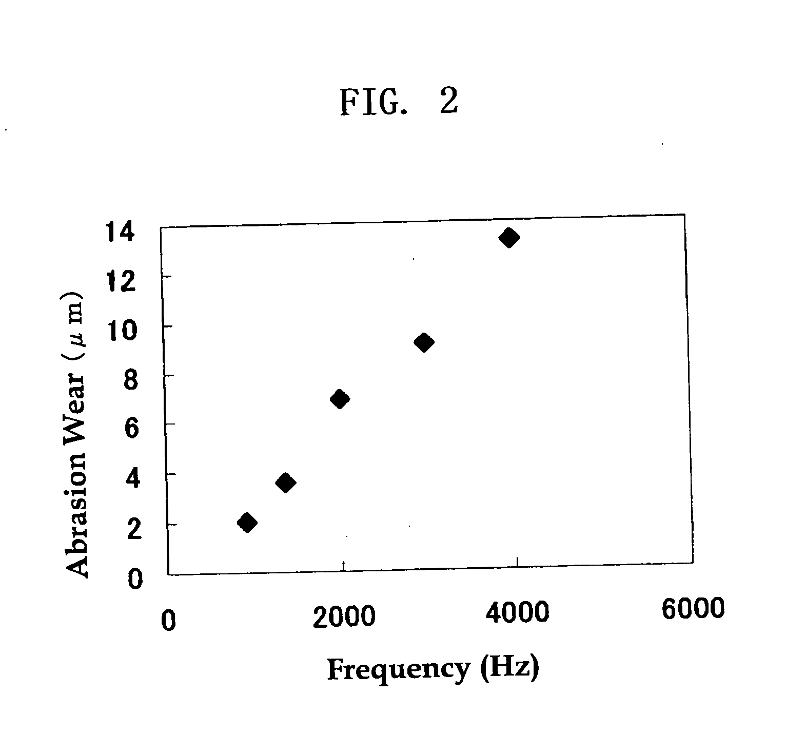
[0034] When the photoconductor is subjected to charging by means of a charging member of roller-like shape, the superimposed AC may improve the charging uniformity. In the charging process, the photoconductor takes place abrasion wear in higher rate while the repeated usage compared to DC charging as known previously. However, the reason has not been understood sufficiently.
[0039] It is known that the wearing of the photoconductor in the image forming apparatus is caused mainly by mechanical stress due to a cleaning member. Various countermeasures have been made for the stress through constructing variously the surface layer such as charge-transporting layer or surface-protective layer of the photoconductor; for example, increasing the molecular weight of the binder resin to promote the entanglement of backbone, using the cross-linking polymer to suppress the defect of molecular chain, using polymer as charge-transporting material to decrease lower molecular weight components as low as possible, and using filler to enhance the mechanical strength. However, these countermeasures are designed on condition that the material employed at the surface layer does not undergo the changes of structure and / or composition even after the repeated usage.
[0041] From these facts, the reason why the abrasion wear of the photoconductor at AC charging is higher than that at DC charging is that the chemical degradation is more significant at AC charging compared to at DC charging, consequently, the mechanical strength is considerably decreased.
[0050] Further, we found that a charging hazard absorber is supplied and the photoconductor surface is coated when the photoconductor is subjected to charging with AC duplication, the degradation of the photoconductor surface may be suppressed without the direct collision of ions against the photoconductor surface.
[0052] As such, although the charging hazard absorber acts to prevent the photoconductor surface from the degradation due to the charging hazard, it may interfere the essential performance i.e. the image forming of image forming apparatus, when the usage is inappropriate, in spite that it may protect the photoconductor surface; the optimization of the charging hazard amount is recognized to be important. We have founded that the conditions may be determined by obtaining the charging hazard amount through the simultaneously variable simulation of AC conditions and by controlling the charging hazard amount, without losing the photoconductor protective performance and without affecting the resulting images, thereby the present invention has been completed.
Problems solved by technology
However, the reason has not been understood sufficiently.
Method used
View moreImage
Smart ImageViewing Examples

Examples
example 1
[0425] Except for changing the charging conditions as follows, evaluations were carried out in the same manner as Comparative Example 1. The results are shown in Table 1-1. [0426] Vdc: −600 V, Vpp: 2200 V, Frequency: 1350 Hz
example 2
[0427] Except for changing the charging conditions as follows, evaluations were carried out in the same manner as Comparative Example 1. The results are shown in Table 1-1. [0428] Vdc: −600 V, Vpp: 2200 V, Frequency: 1600 Hz
example 3
[0429] Except for exchanging the charging conditions as follows, evaluations were carried out in the same manner as Comparative Example 1. The results are shown in Table 1-1. [0430] Vdc: −600 V, Vpp: 2200 V, Frequency: 2000 Hz
Login to View More PUM
 Abstract
The present invention relates to an image forming apparatus, an image forming process and a process cartridge, in which the image quality and the durability of the photoconductor may be enhanced, images may be formed stably even after the repeated usages, and higher quality and higher stability of images may be established due to the superimposed alternating voltage as well as decrease of the charging hazard on the photoconductor. Specifically, the image forming apparatus according to the present invention comprises a photoconductor, latent electrostatic image forming unit, developing unit a transferring unit, and fixing unit, wherein, the charging member is of roller shape disposed proximate to the photoconductor, the photoconductor is charged at the charging nip portion formed between the photoconductor and the charging member, in a condition that satisfies the following Equation: 4.4×10¹⁴≦[(Number of Charged Particles)÷(Perimeter of Photoconductor)]≦17.7×10¹⁴ [0001]wherein the “Number of Charged Particles” refers to the number of charged particles accepted by the photoconductor surface per its unit surface area from the operated charging member, while the photoconductor rotates one round, thus the unit is [number / m2]; and the unit of “Perimeter of Photoconductor” is [mm].
Description
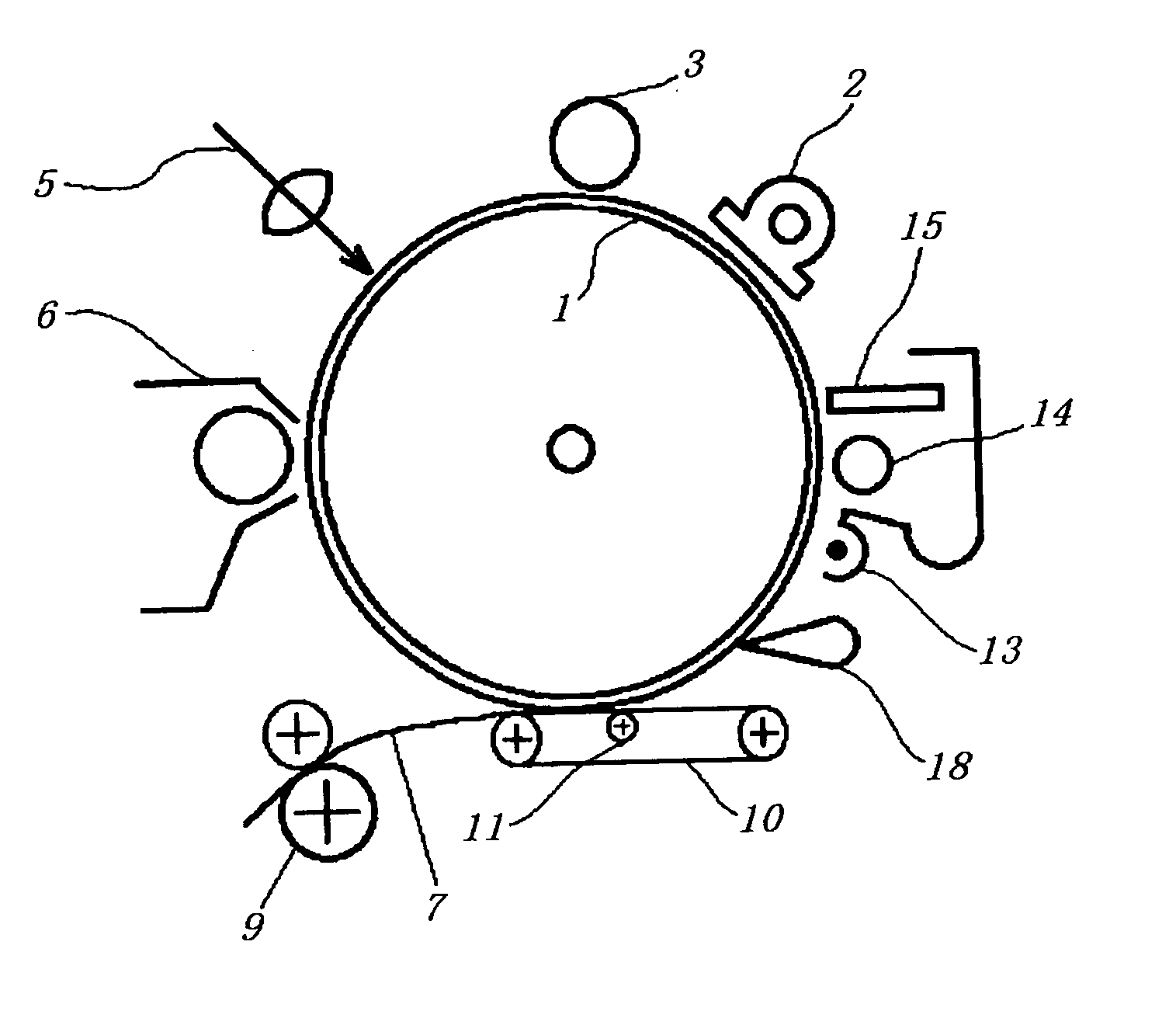
BACKGROUND OF THE INVENTION [0002] 1. Field of the Invention [0003] The present invention relates to an image forming apparatus, an image forming process and a process cartridge, in which an alternating voltage is superimposed on a direct voltage and the voltage is applied to a charging member of roller-shape disposed proximity to a photoconductor, then the photoconductor is charged and an image is formed. More specifically, the present invention relates to an image forming apparatus, an image forming process and a process cartridge, in which the image quality and the durability of the photoconductor may be enhanced, images may be formed stably even after the repeated usages, and higher quality and higher stability of images may be established due to the superimposed alternating voltage as well as decrease of the charging hazard on the photoconductor. [0004] 2. Description of the Related Art [0005] An image forming apparatus is typically constituted from a photoconductor (hereinafte...
Claims
Login to View More Application Information
Patent Timeline
 IPC IPC(8): G03G5/06G03G5/07G03G5/043G03G5/14G03G5/147G03G15/02G03G21/00G03G21/18
CPCG03G2215/02G03G15/0266
InventorNIIMI, TATSUYAKADONAGA, MASAMI
OwnerRICOH KK