Electronic circuit designing method and apparatus, and storage medium

a technology of electronic circuits and circuits, applied in the direction of cad circuit design, program control, instruments, etc., can solve the problems of increasing the design time, and affecting the design quality of the circui

Inactive Publication Date: 2005-04-21
FUJITSU LTD
View PDF33 Cites 16 Cited by
  • Summary
  • Abstract
  • Description
  • Claims
  • Application Information

AI Technical Summary

Benefits of technology

[0008] Accordingly, it is a general object of the present invention to provide a novel and useful electronic circuit designing method, electronic circuit designing apparatus and computer-readable storage medium, in which the problems described above are eliminated.
[0009] Another and more specific object of the present invention is to provide an electronic circuit designing method, an electronic circuit designing apparatus and computer-readable storage medium, which can eliminate the first problem and / or the second problem described above.
[0036] According to the present invention, it is possible to design the electronic circuit so that the quality of the circuit design is not greatly dependent upon the degree of skill of the circuit designer and / or to prevent the design time from increasing due to repetition of the operation of reviewing the design constraints.

Problems solved by technology

For this reason, there is a first problem in that the design quality of the circuit is greatly dependent on the skill of the circuit designer.
In other words, the design quality becomes inconsistent depending on the skilled level of the circuit designers, and the design time increases due to design corrections which need to be made depending on the skilled level of the circuit designer.
However, such an operation of looking over the design constraints needs to be repeated many times in most cases, and there is a second problem in that the deign time is considerably increased thereby.

Method used


Image

  • Electronic circuit designing method and apparatus, and storage medium
  • Electronic circuit designing method and apparatus, and storage medium
  • Electronic circuit designing method and apparatus, and storage medium

Examples


Embodiment Construction

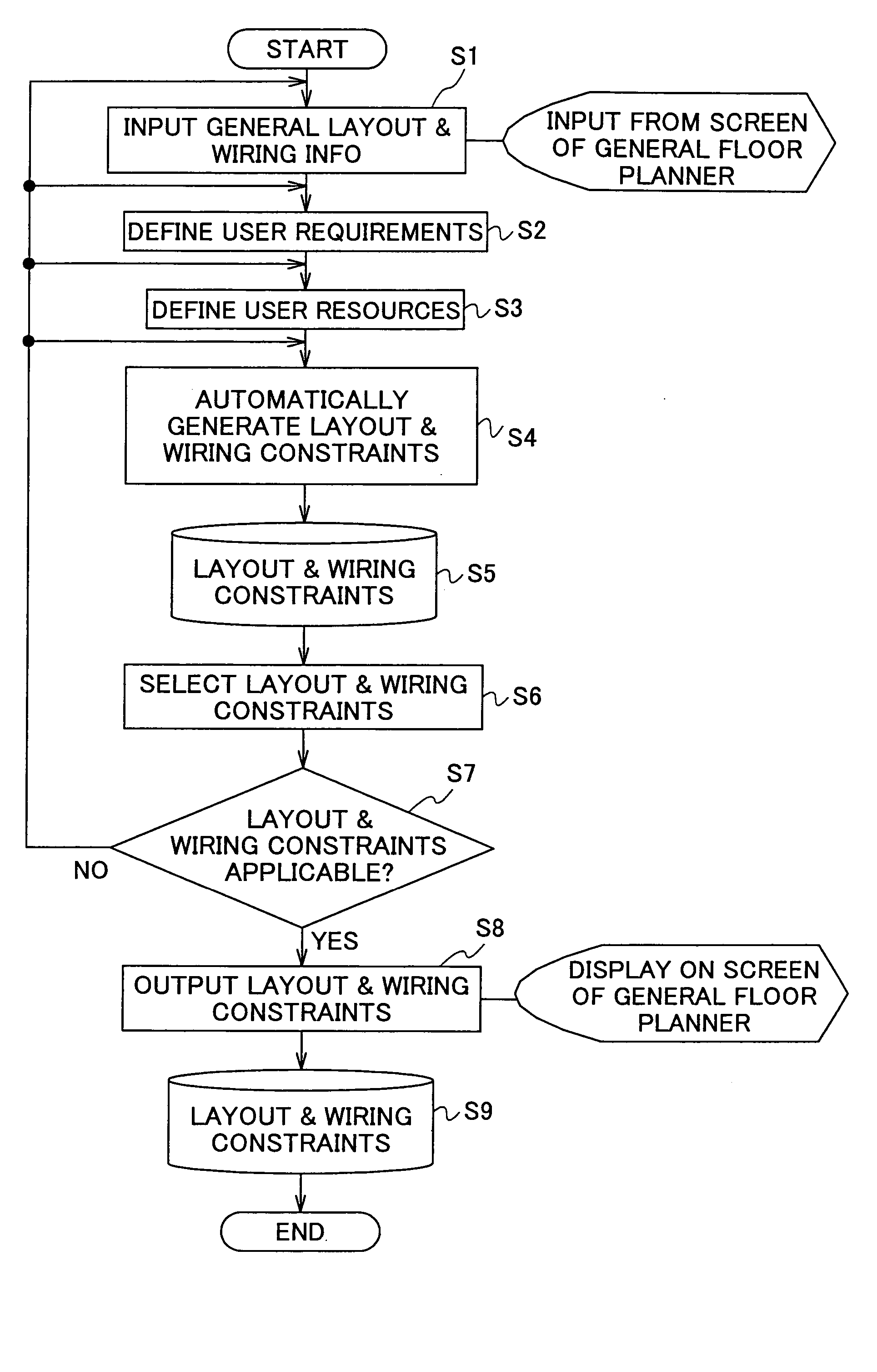
[0084] A description will be given of various embodiments of an electronic circuit designing method according to the present invention, an electronic circuit designing apparatus according to the present invention, and a computer-readable storage medium according to the present invention, by referring to the drawings.

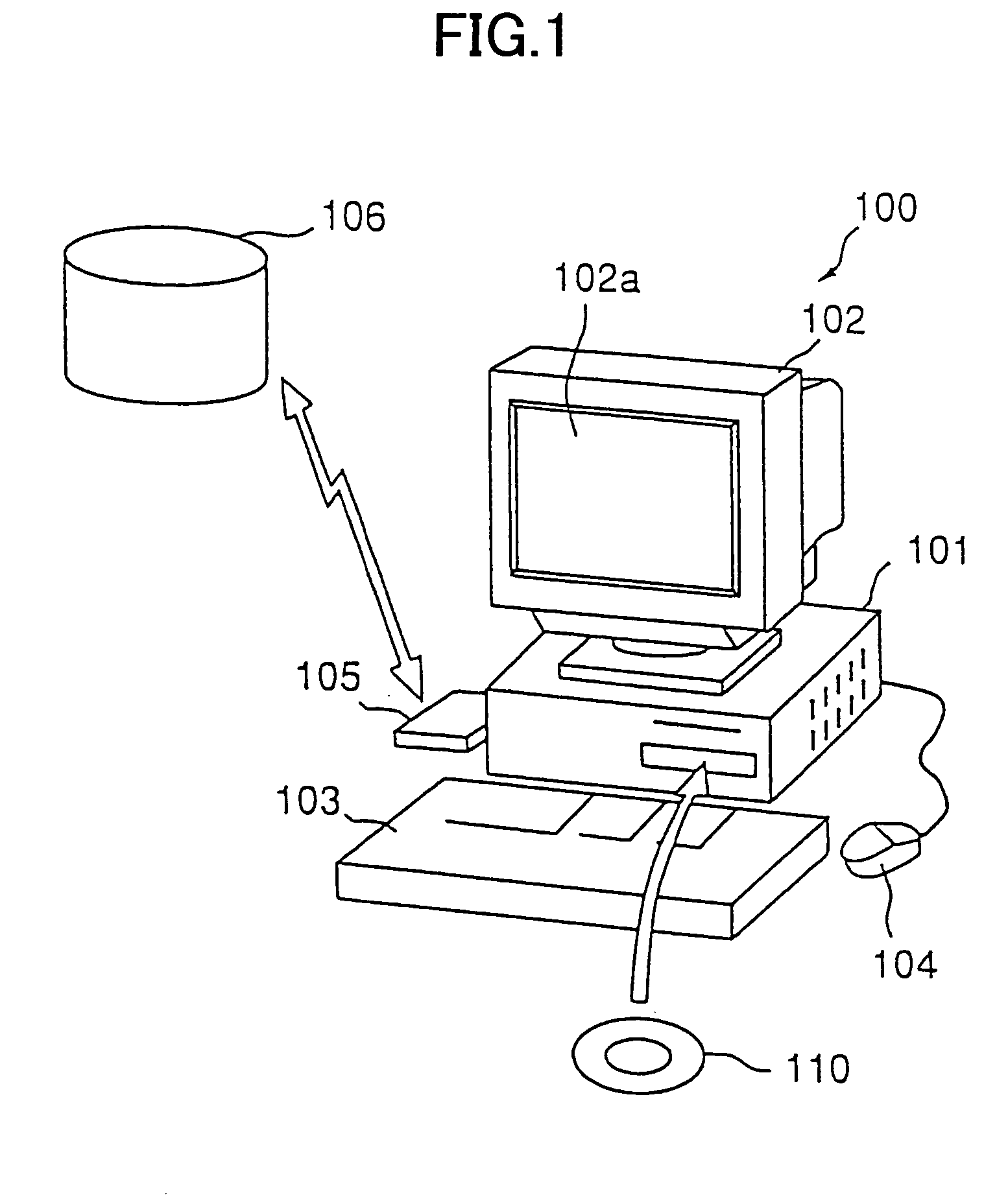
[0085] First, a description will be given of an embodiment of the electronic circuit designing apparatus according to the present invention. This embodiment of the electronic circuit designing apparatus employs an embodiment of the electronic circuit designing method according to the present invention and an embodiment of the computer-readable storage medium according to the present invention. In this embodiment, the present invention is applied to a computer system. FIG. 1 is a perspective view showing the computer system applied with the present invention in this embodiment.

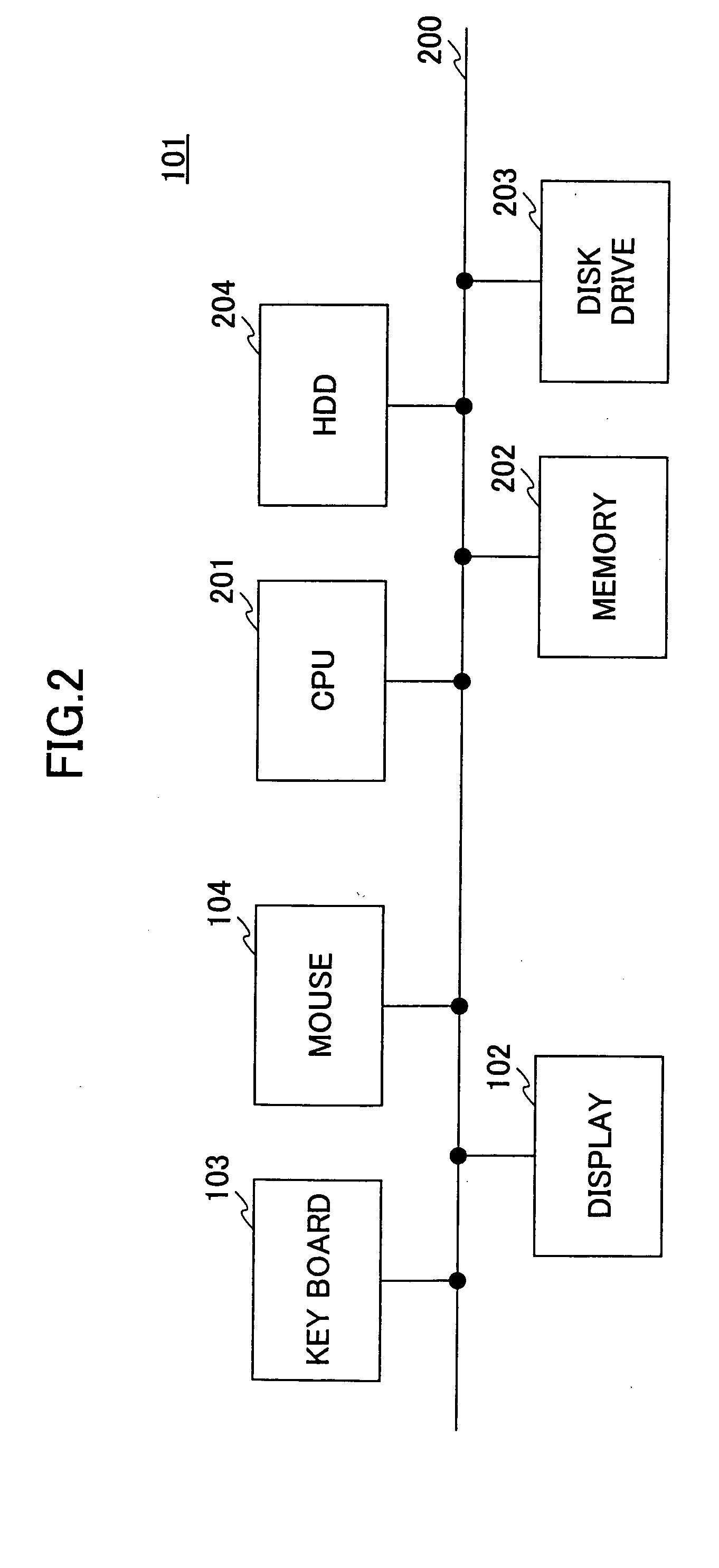
[0086] A computer system 100 shown in FIG. 1 generally includes a main body 101 which includes...


PUM


Abstract

An electronic circuit designing method and apparatus designs an electronic circuit by CAD, by generating design constraints with respect to the electronic circuit based on at least one of general layout and wiring information related to devices and wirings included in the electronic circuit, user requirements defined by a user, and user resources defined by the user, and urging an input to the user by displaying the design constraints.

Description

BACKGROUND OF THE INVENTION [0001] This application claims the benefit of Japanese Patent Applications No. 2001-210671 filed Jul. 11, 2001 and No. 2002-101646 filed Apr. 3, 2002, in the Japanese Patent Office, the disclosures of which are hereby incorporated by reference. [0002] 1. Field of the Invention [0003] The present invention generally relates to electronic circuit designing methods and apparatuses and storage media, and more particularly to an electronic circuit designing method and an electronic circuit designing apparatus for designing an electronic circuit such as large scale integrated circuits (LSIs), multi chip modules (MCMs) and printed circuit boards (PCBs), and to a computer-readable storage medium which stores a program for causing a computer to carry out such a designing of the electronic circuit. [0004] 2. Description of the Related Art [0005] When designing an electronic circuit using computer-aided design (CAD), the design procedure includes a first step which ...

Claims


Application Information

Patent Timeline
Patent Type & Authority Applications(United States)
IPC IPC(8): G06F17/50H01L21/82
CPCG06F17/5045G06F17/5036G06F30/30G06F30/367
Inventor SATO, TOSHIROKOBAYASHI, KAZUMASAFUJIMORI, SHOGO
Owner FUJITSU LTD
Why Eureka
Try Eureka