Method and system for automatic stress analysis of analog components in digital electronic circuit

an electronic circuit and stress analysis technology, applied in the field of automatic stress analysis of analog components in digital electronic circuits, can solve the problems of undue complexity or gross oversimplification, hdl simulations, failure to test or verify the operation of discrete analog components simulation and stress analysis tools available for analog simulation and analysis cannot be applied presently for discrete analog components embedded in digital electronic circuit designs, etc., to achieve accurate and comprehensive analysis

Active Publication Date: 2012-03-27
CADENCE DESIGN SYST INC
View PDF6 Cites 15 Cited by
  • Summary
  • Abstract
  • Description
  • Claims
  • Application Information

AI Technical Summary

Benefits of technology

[0019]A primary object of the present invention is to provide a method and system whereby the stress to be encountered

Problems solved by technology

Similar techniques for the automatic testing and/or verification of analog components discretely embedded in digital design are not heretofore known, however, at least not without either undue complexity or gross oversimplification.
These HDL simulations, however, fail to test or verify the operation of the circuit's discretely embedded analog components.
The simulation and stress analysis tools available for analog simulation and analysis cannot be applied presently for discrete analog components which are embedded in digital electronic circuit designs.
Not only are HDL models very difficult to fully obtain for board level simulation, the modeling of supplemental interface elements (such as analog-to-digital and digital-to-analog converters) is also required to facilitate the mix-signal simulation that would occur.
These and other obstacles make the co-simulation techniques known in the art prohibitively expensive for most applications, both in cost and computational load.
Circuit designers are often relegated, therefore, to manual c

Method used


Image

  • Method and system for automatic stress analysis of analog components in digital electronic circuit
  • Method and system for automatic stress analysis of analog components in digital electronic circuit
  • Method and system for automatic stress analysis of analog components in digital electronic circuit

Examples


Embodiment Construction

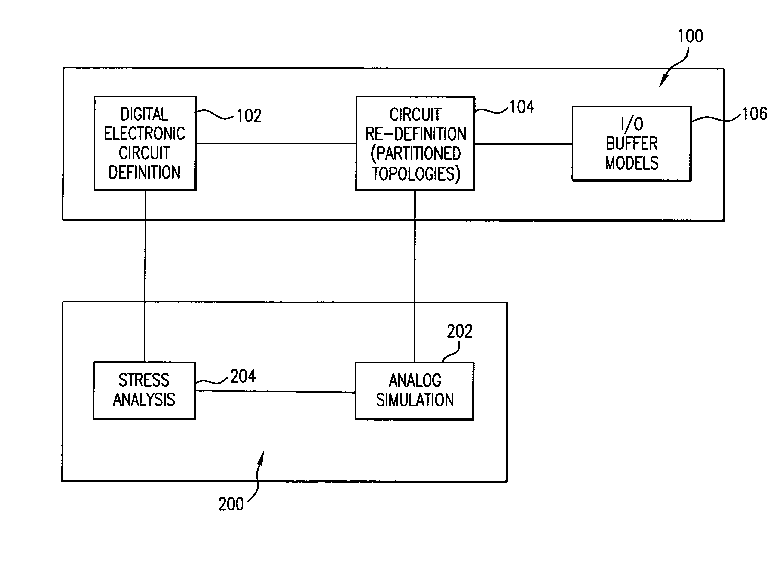
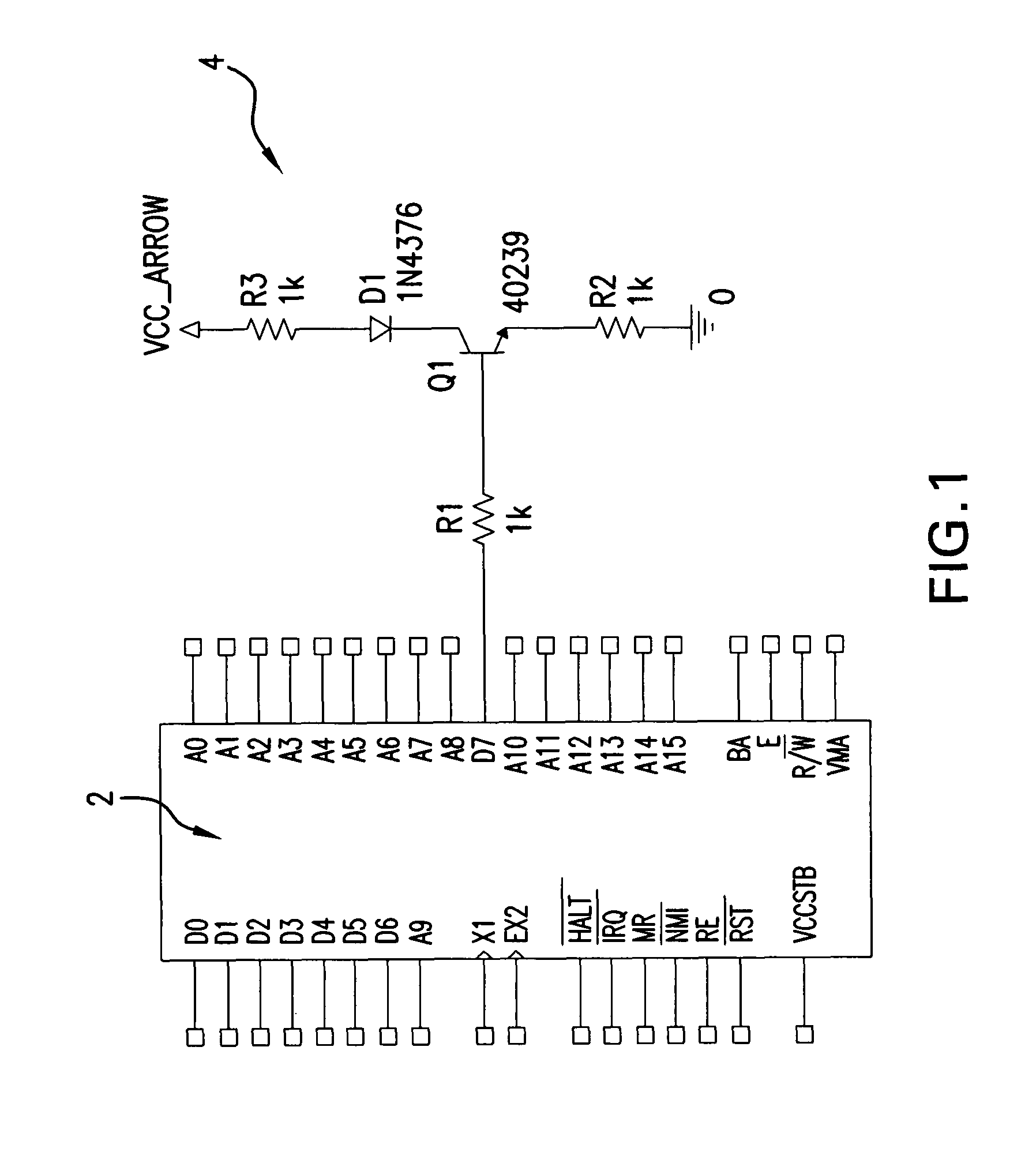
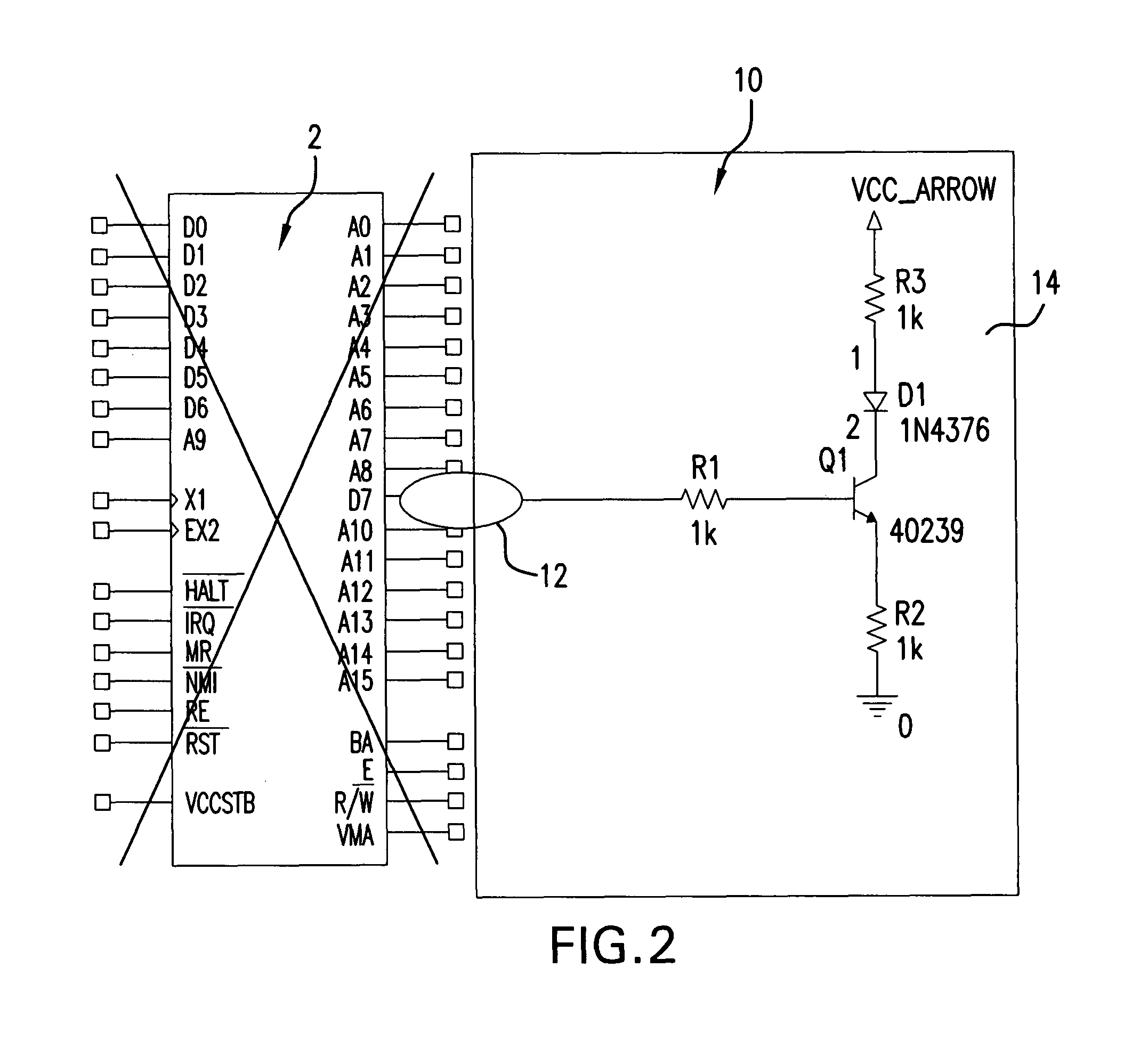
[0033]As used herein, the term maximum operating condition (MOC) refers to the extreme levels potentially encountered during operation for various operational parameters such as “maximum temperature,”“maximum power-dissipation,” and the like. The term technology used in connection with a particular device refers to “ECL,”“LSTTL,”“CMOS,” or other such classifications known in the art relating to the physics of the device. The term analog topology refers to a particular portion of the given electronic circuit sufficiently self-contained that it may be treated for simulation purposes in a manner independent of the other circuit portions, and which preferably terminates at a digital device (or an IO buffer representation thereof), a bias point (for example VCC or ground), or a floating node.

[0034]In accordance with one aspect of the present invention, an automated approach is realized whereby stress measurements for analog components embedded within digital electronic circuit designs ma...


PUM


Abstract

An automated approach is provided for evaluating stress upon analog components embedded in a digital electronic circuit design. The approach includes establishing a computer readable circuit definition of the digital electronic circuit design. The circuit definition is then partitioned into a plurality of circuit portions, which are re-defined to form a plurality of analog topologies. The analog topologies are adapted for automatic analog simulation one independent of the other, with all digital components substituted by at least one subcircuit including instantiation of a corresponding input output (IO) buffer model. Automatic analog simulation is carried out upon the analog topologies to generate simulated results data, which are automatically postprocessed to generate worst-case stress measurement data for one or more critical components identified in the analog topologies.

Description

BACKGROUND OF THE INVENTIONField of the Invention[0001]The subject method and system for automatic stress analysis of analog components in a digital electronic circuit is generally directed to the optimization of a digital electronic circuit design prior to physical implementation. More specifically, the method and system provides automatic estimates of the actual ‘stress’ that analog components embedded in a digital electronic circuit would be subjected to during actual operation, so as to enhance the circuit's reliable operation upon physical implementation in a printed circuit board (PCB) or the like.[0002]In carrying out such physical electronic circuit implementations as PCBs, the desired electronic circuit is schematically defined once it is conceptually designed. For digital electronic circuits, this schematic definition invariably includes not only pre-packaged integrated circuit (IC) devices with manufacturer-defined interconnection pins, but also discretely embedded analog...

Claims


Application Information

Patent Timeline
IPC IPC(8): G06G7/48
CPCG06F17/5036G06F30/367
Inventor KUKAL, TARANJIT SINGHDHARMARAJAN, SANKARAN
Owner CADENCE DESIGN SYST INC
Why Eureka
Try Eureka