Automatic insertion of clocked elements into an electronic design to improve system performance

a technology of electronic design and clock element, applied in the direction of computer aided design, instrumentation, cad circuit design, etc., can solve the problems of increasing the ratio of wire delay to gate delay, communication can now take much longer than the clock cycle required, and is not a feasible alternative for high-performance designs. , to achieve the effect of optimizing system performance and improving performan

Active Publication Date: 2007-04-17
CADENCE DESIGN SYST INC
View PDF19 Cites 15 Cited by
  • Summary
  • Abstract
  • Description
  • Claims
  • Application Information

AI Technical Summary

Benefits of technology

[0008]Methods for inserting clocked elements into electronic designs to improve their performance provide a way to indicate where clocked elements might be inserted, and the cost of doing so. A placer, or a synthesis tool incorporating a placer, can then decide which of these locations should be used, and how many clocked elements should be inserted at each location, in order to either make the design feasible or to optimize system performance. The tool can communicate the resulting design to a designer and other tools.

Problems solved by technology

As electronic circuit manufacturing processes shrink, the ratio of wire delay to gate delay keeps increasing.
This communication can now take much longer than the clock cycle required for even a relatively complex local operation.
This may work for applications that are intended for optimizing high density or low power concerns, but it is not a feasible alternative for high performance designs.
However, this has several problems.
A latency-insensitive design does not help performance in the case of significant wire delay.
However, most IP is not available in latency insensitive, much less asynchronous, forms.
Even if a latency insensitive design works with any combination of delays, some delay combinations may be much faster than others.
Designers are unable to determine which combinations have less delay than others, so optimizing the design to reduce latency is a problem.
Even though this technique is highly effective, it is seldom used.
The main reason is that pipelining the interconnect changes the cycle level behavior, which requires a large variety of manual rework of the design, for which there is very little tool support.
Inserting clocked elements into a design is difficult and time consuming, because only some locations of the design are legal for this operation.
Automatic tools, such as placers and synthesis tools, are unable to determine locations where the designer could insert clocked elements.
Furthermore, the impact of inserting clocked elements into the design is difficult for tools to determine.
For example, there are no tools that attempt to optimize the placement and potential insertion of clocked elements.
The results of any insertion decisions should be communicated to the designer and other tools, however, no tools currently exist to automate this process.
Theoretically, then, design roadmaps could assume that designers will use interconnect pipelining to estimate an achievable clock speed for a microprocessing unit (MPU), but they fail to provide a practical method of automatically performing the pipelining during the design process.
Consequently, designers seldom use interconnect pipelining at all because of the logistical difficulty of using conventional methods.
For example, users rarely try different pipeline schemes since adding or deleting the flip-flops by hand is too hard.

Method used


Image

  • Automatic insertion of clocked elements into an electronic design to improve system performance
  • Automatic insertion of clocked elements into an electronic design to improve system performance
  • Automatic insertion of clocked elements into an electronic design to improve system performance

Examples


Embodiment Construction

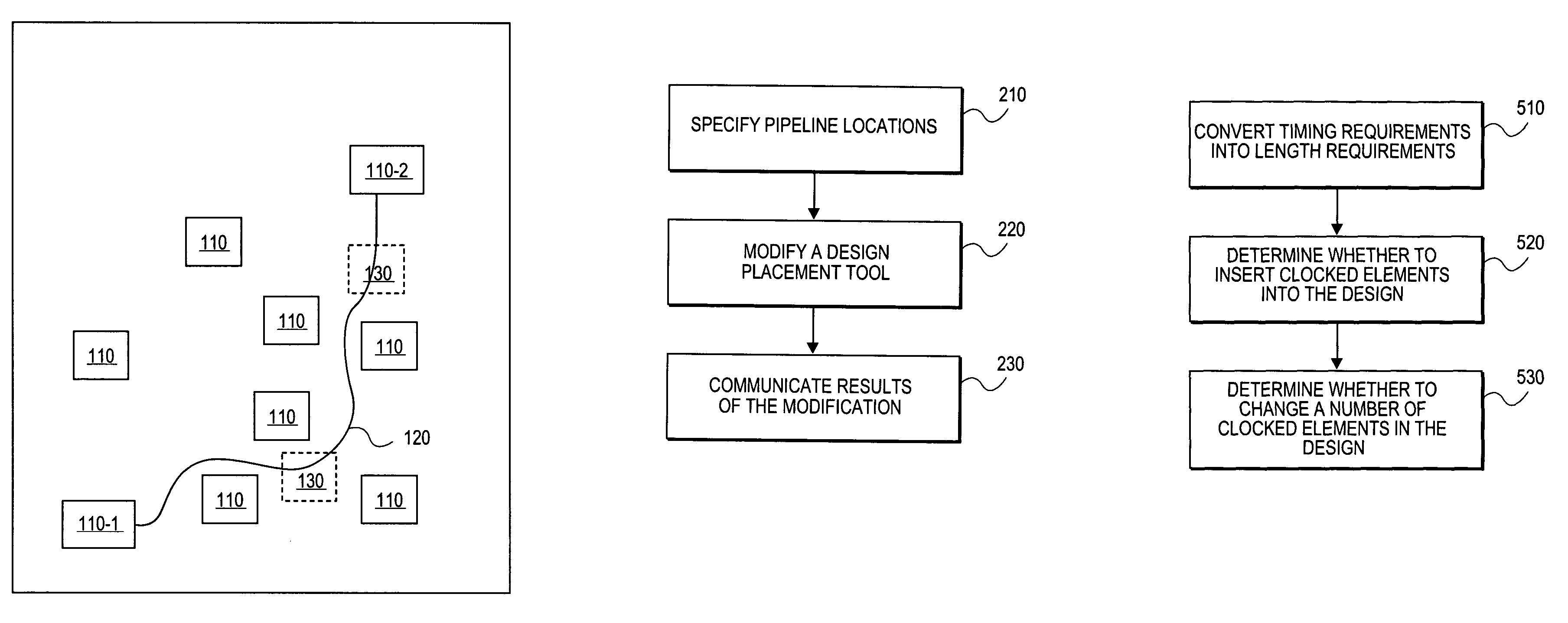
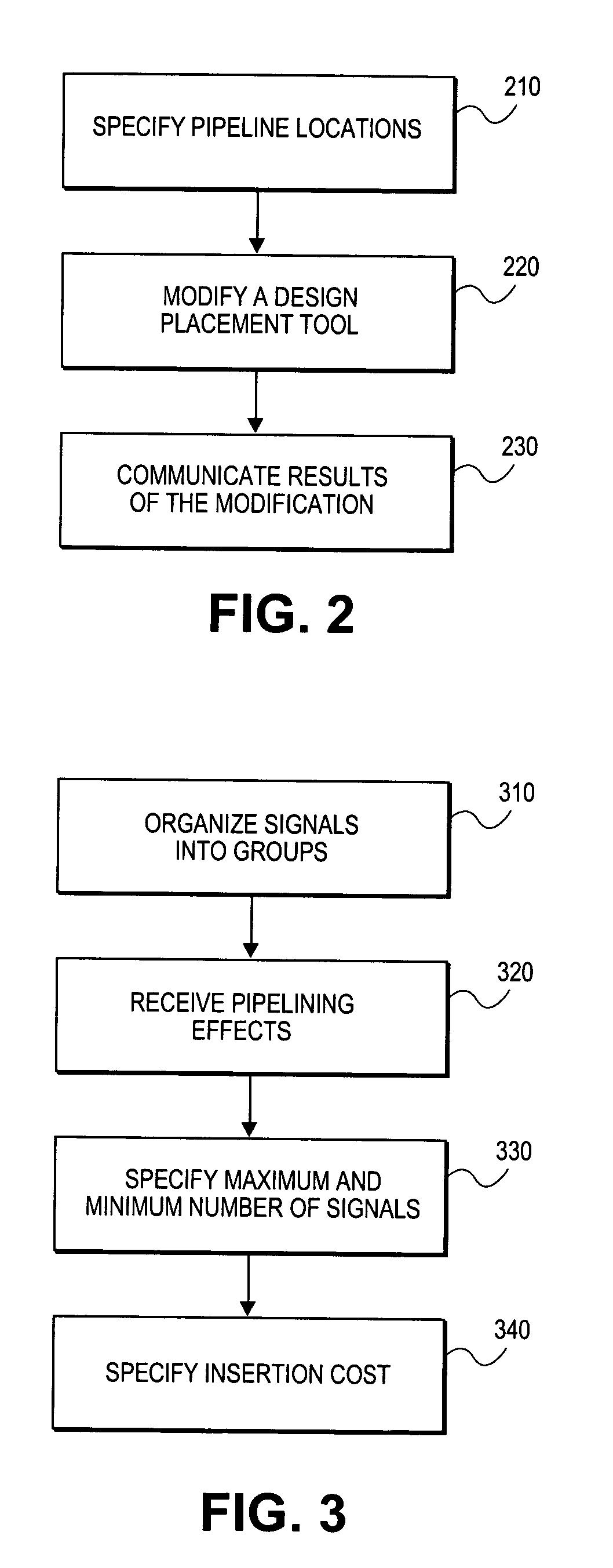
[0016]To perform interconnect pipelining, either the user or an appropriate computer-implemented process specifies, to an automated tool, where it is possible to insert clocked elements such as flip-flops or latches, and specifies the impact of using each possible location. With this information, and in combination with the design's physical layout, the automated tool can choose which signals may benefit from additional stages. After insertion, information about inserted clocked elements are communicated to the designers and other tools in the design flow.

[0017]To create the pipeline, the impact of pipelining a given signal is considered. The signal's impact may vary greatly, depending on the importance of that signal to the overall system performance. For some signals, pipelining may adversely affect system performance. Avoiding pipelining may be a default mode for one or more signals, and can remain true where the highest performance is needed. For some signals, pipelining is free...


PUM


Abstract

A method of improving a design of an electronic circuit includes generating the design, specifying one or more pipeline locations of the design, modifying the one or more pipeline locations of the design, and communicating the results to a user.

Description

CROSS-REFERENCE TO RELATED APPLICATION[0001]This application claims the benefit of U.S. Prov. No. 60 / 410,515 filed Sep. 13, 2002, which is incorporated herein by reference in its entirety.BACKGROUND OF THE INVENTION[0002]As electronic circuit manufacturing processes shrink, the ratio of wire delay to gate delay keeps increasing. An integrated circuit (IC), or chip, has operations where distant parts of the chip communicate with each other. This communication can now take much longer than the clock cycle required for even a relatively complex local operation. To address this issue, designers can run the entire design at the speeds determined by the slowest global interconnect, or run the design at one speed and the global interconnect at a different (slower) speed. Acceptance of the fact that global signals can be clocked more slowly than local signals was used in the design of the previous International Technology Roadmap for Semiconductors (ITRS) roadmaps, which distinguished betwe...

Claims


Application Information

Patent Timeline
Patent Type & Authority Patents(United States)
IPC IPC(8): G06F17/50H01L
CPCG06F17/5045G06F30/30
Inventor SCHEFFER, LOUIS K.
Owner CADENCE DESIGN SYST INC
Why Eureka
Try Eureka