Ball grid array package and method thereof

a technology of grid array and ball, applied in the direction of resist details, printed circuit aspects, printed circuit manufacturing, etc., can solve the problems of increasing manufacturing processes and costs, and achieve the effect of preventing flux from spreading and increasing the implantation yield of solder balls

Inactive Publication Date: 2005-04-28
ADVANCED SEMICON ENG INC
View PDF6 Cites 5 Cited by
  • Summary
  • Abstract
  • Description
  • Claims
  • Application Information

AI Technical Summary

Benefits of technology

[0013] According to the BGA package of the present invention, the plurality of partitioning walls can prevent the flux from spreading and therefore avoid the solder bridge being formed betw

Problems solved by technology

However, the plurality of groove mounting pads wi

Method used


Image

  • Ball grid array package and method thereof
  • Ball grid array package and method thereof
  • Ball grid array package and method thereof

Examples


Embodiment Construction

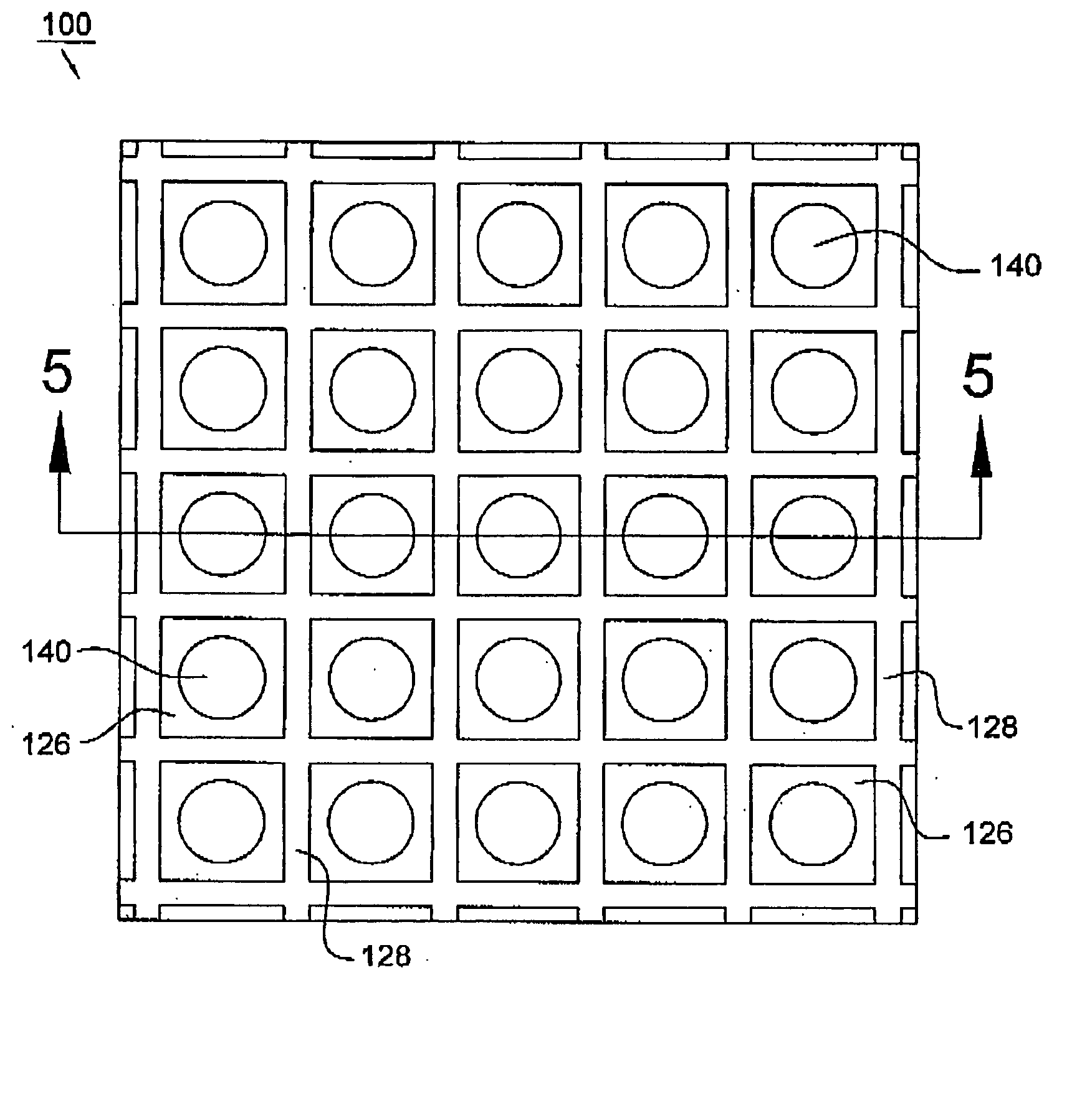
[0020]FIGS. 4 and 5 show a ball grid array (BGA) package 100 according to one embodiment of the present invention. The BGA package 100 includes a substrate 120 and a chip 111. The substrate 120 has an upper surface 122, a lower surface 124 opposite to the upper surface, and a plurality of wirings (not shown). The chip 111 is disposed on the upper surface 122 of the substrate 120 and electrically connected to the wirings of the substrate through bonding wires, that is, the chip 111 is electrically connected to the substrate by wire bonding technique. A package body is formed over the chip 111 and a portion of the upper surface 122 of the substrate 120. It should be understood by a skilled person in art that the chip 111 can be replaced by a flip chip.

[0021] A plurality of pads 150 are disposed on the lower surface 124 of the substrate 120 and electrically connected to the chip 111 through the wirings. A plurality of solder balls 140 are respectively disposed on the plurality of pads...


PUM


Abstract

A ball grid array package includes a substrate, a chip, a plurality of pads, a solder mask, a plurality of partitioning walls, and a plurality of solder balls. The substrate has an upper surface and a lower surface opposite to the upper surface. The chip is disposed on the upper surface of the substrate. The pads are disposed on the lower surface of the substrate and electrically connected to the chip. The solder mask is disposed on the lower surface of the substrate. The partitioning walls are disposed on the solder mask and between the adjacent pads. The solder balls are respectively disposed on the pads.

Description

[0001] This application claims the priority benefit of Taiwan Patent Application Serial Number 092129954, filed Oct. 28, 2003, the full disclosure of which is incorporated herein by reference. BACKGROUND OF THE INVENTION [0002] 1. Field of the Invention [0003] This invention generally relates to a ball grid array package, and more particularly to a ball grid array package having a plurality of partitioning walls for keeping solder balls in proper position. [0004] 2. Description of the Related Art [0005] Miniaturization of semiconductor device size has been an important topic in the art, when the device requires more I / O pins along with the increase of device density. Relatively, the ball grid array (BGA) package is an efficient packaging technology since it can provide more I / O pins. [0006] Referring to FIG. 1, it shows a conventional ball grid array (BGA) package 10 using wire bonding technique and being disposed on a main board 30. The BGA package 10 includes a substrate 20, a chi...

Claims


Application Information

Patent Timeline
IPC IPC(8): H01L21/48H01L23/31H01L23/48H01L23/498H05K3/34
CPCH01L21/4853H01L23/49816H01L2224/48091H01L2224/48227H01L2924/15311H01L24/48H05K3/3452H05K2201/10734H05K2203/0588H05K3/3436H01L2924/00014H01L2924/181
Inventor LIU, SHENG TSUNG
Owner ADVANCED SEMICON ENG INC
Why Eureka
Try Eureka