Plasma display apparatus
- Summary
- Abstract
- Description
- Claims
- Application Information
AI Technical Summary
Benefits of technology
Problems solved by technology
Method used
Image

Examples
first embodiment
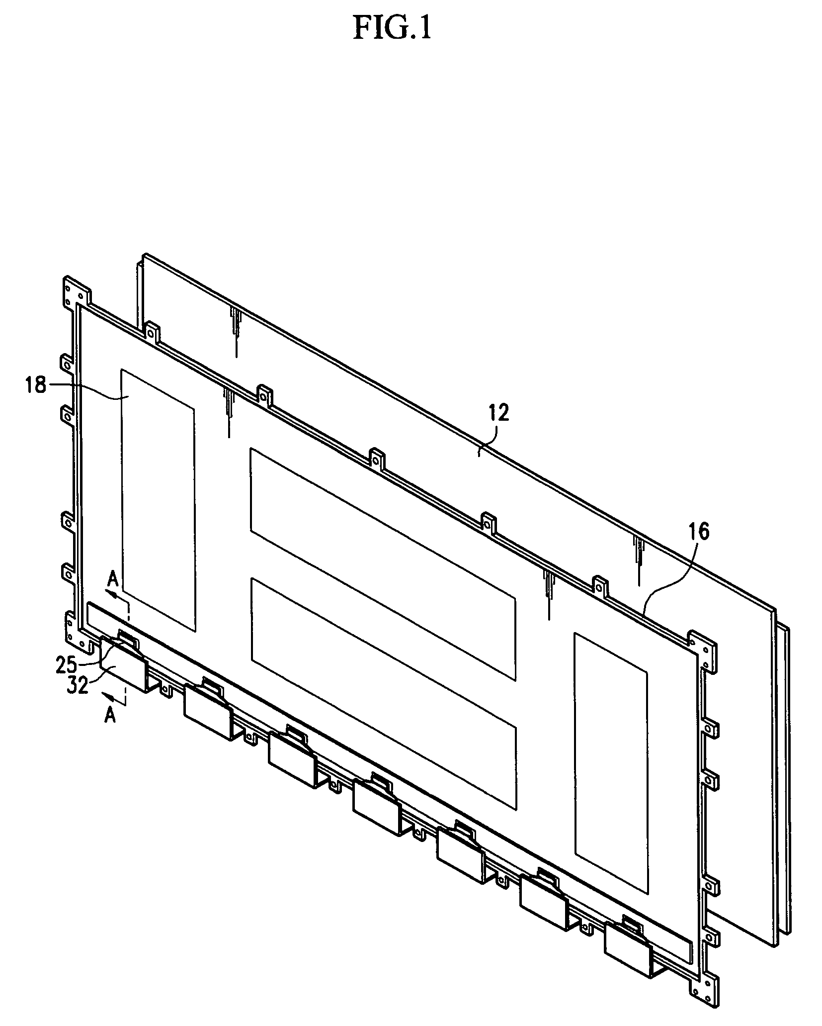
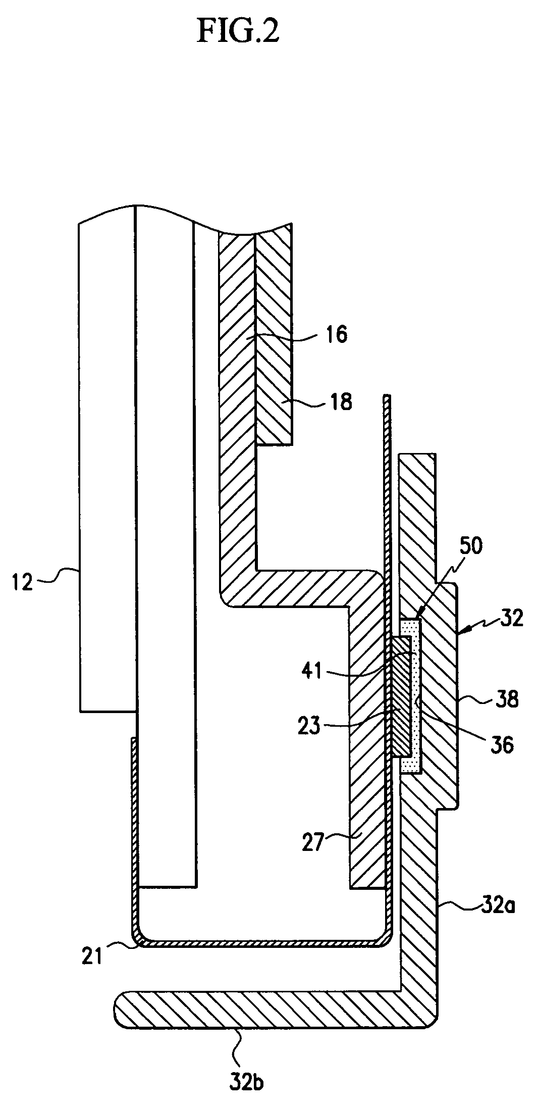
[0046]FIG. 1 is an exploded perspective view of a plasma display apparatus having a heat dissipating structure for a driver IC according to the present invention, and FIG. 2 is a cross-sectional view taken along the A-A line of FIG. 1.
[0047] With reference to FIG. 1 and FIG. 2, the plasma display apparatus includes a plasma display panel 12 (referred to hereinafter simply as a “PDP”), and a chassis base 16. The chassis base 16 is made of Cu, Fe, or the like, and the PDP 12 is mounted on one side surface thereof and a driving circuit 18 is mounted on the other side surface of the chassis base 16.
[0048] The PDP 12 of the plasma display device is mounted on a chassis base (not shown), with a front cover (not shown) on the outside of the PDP 12 and a rear cover (not shown) on the outside of a chassis base.
[0049] Electrodes extending from the periphery of the PDP 12 are electrically connected to the driving circuit 18 to receive the signals required for driving the PDP 12.
[0050] A dri...
second embodiment
[0065]FIG. 3 is a cross-sectional view of a heat dissipating structure for a driver IC according to the present invention.
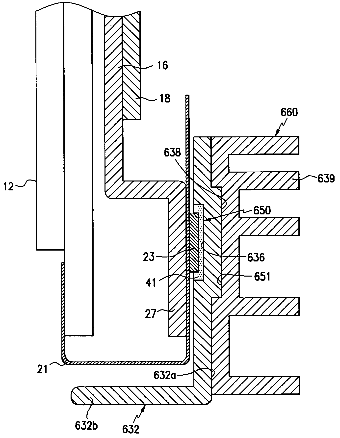
[0066] With reference to FIG. 3, unlike the first embodiment, a heat dissipating plate 132 is provided with only a first portion 132a opposite to the driver IC 23. An accommodating portion 150 is provided with an accommodating recess 136 formed on the one side surface of the first portion 132a, and a projecting portion 138 formed outwardly from the other side surface thereof and corresponding to the accommodating recess 136. The width and height of the projection portion 138 is determined according to the width and depth of the accommodating recess 136.
[0067] As a result, since the heat dissipating plate 132 according to the second embodiment excludes the second portion 32b of FIG. 2, the total size of the plasma display apparatus and the material used for forming the heat dissipating plate are reduced, thereby resulting in a more compact and simplified plasma d...
third embodiment
[0068]FIG. 4 is a cross-sectional view of a heat dissipating structure for a driver IC according to the present invention.
[0069] With reference to FIG. 4, an accommodating recess 250 of a heat dissipating plate 232 has a “”-shaped cross-section with an interior accommodating portion 236, and the heat dissipating plate 232 thereof is recessed and is fitted to the chassis base 16 so that it accommodates the thermal conductive medium 41 and the entire driver IC 23. Accordingly, the heat generated by the driver IC is effectively transferred to the heat dissipating plate 232 through the thermal conductive medium 41.
[0070]FIG. 5 is a cross-sectional view of a heat dissipating structure for a driver IC 23 according to the forth embodiment of the present invention.
[0071] With reference to FIG. 5, a heat dissipating plate 332 is constructed such that it is provided with an accommodating portion 350 having a cavity 336 on the interior thereof so as to surround the entire driver IC 23 and at...
PUM
 Abstract
Description
Claims
Application Information
 - Generate Ideas
- Intellectual Property
- Life Sciences
- Materials
- Tech Scout
- Unparalleled Data Quality
- Higher Quality Content
- 60% Fewer Hallucinations
Browse by: Latest US Patents, China's latest patents, Technical Efficacy Thesaurus, Application Domain, Technology Topic, Popular Technical Reports.
© 2025 PatSnap. All rights reserved.Legal|Privacy policy|Modern Slavery Act Transparency Statement|Sitemap|About US| Contact US: help@patsnap.com