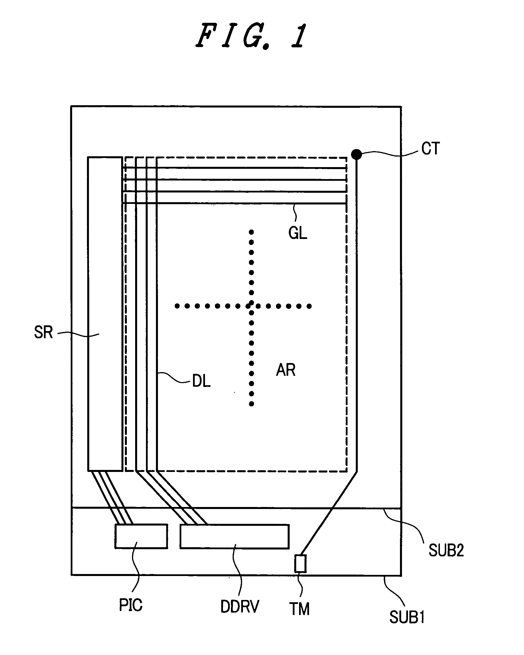
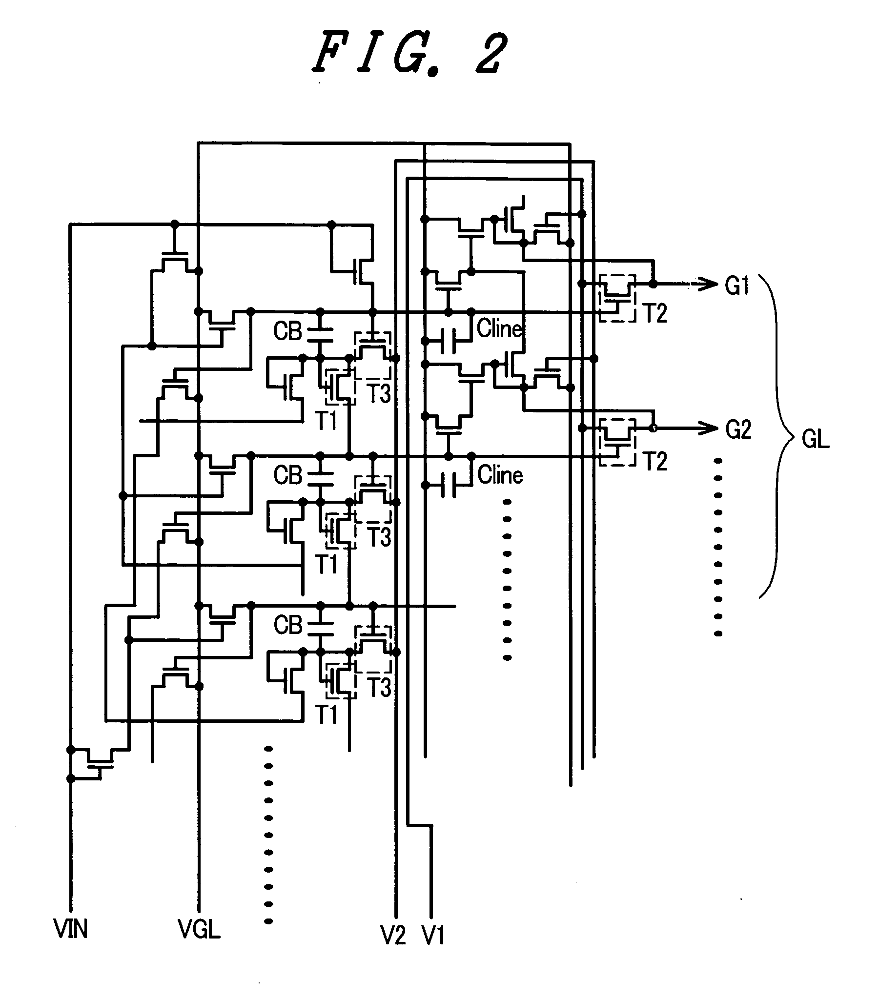
When the channel width is narrowed to achieve the narrowing of the picture frame, this brings about...
Benefits of technology
[0013] Due to such a constitution, even when the channel width is equal, compared to the channels which extend in one direction, the bent channels can decrease an area which the thin film transistors occupy without deteriorating an operational function of the thin film transistor. As a result, it is possible to decrease a built-in area of the gate drive circuit which is arranged on t...
Abstract
The present invention provides a display device having a substrate which includes a display region on which a large number of pixels are arranged in a matrix array and drive circuits which drive the pixels outside the display region, wherein a drive circuit which applies signals to pixel circuits is directly built in the substrate outside the display region. A channel portion of a thin film transistor where a source electrode and a drain electrode face each other in an opposed manner which constitutes a drive circuit is formed in a bent shape which bends on a plane substantially parallel to the substrate.
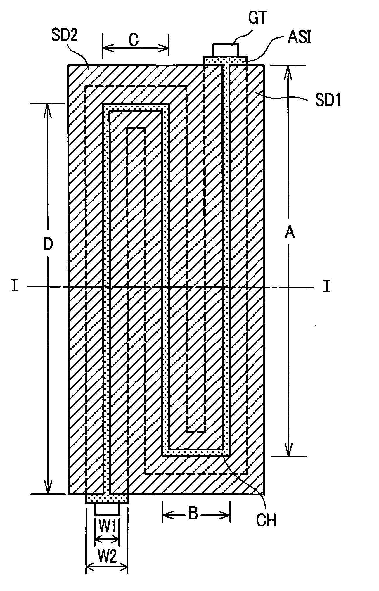
[0035]FIG. 6A is a plan view of a thin film transistor for schematically explaining the embodiment 1 of the display device according to the present invention and FIG. 6B is a cross-sectional view taken along a line I-I in FIG. 6A. In this embodiment, the thin film transistors which constitute the shift register circuit of the gate drive circuit explained in conjunction with FIG. 1 and FIG. 2 or the gate selector circuit of the gate drive circuit explained in conjunction with FIG. 3 and FIG. 4 have the structure shown in FIG. 6A and FIG. 6B.
[0036] In FIG. 6A and FIG. 6B, on the main surface of the glass substrate SUB1 which constitutes the first substrate, first of all, the gate electrode GT is formed by patterning in a state that the gate electrode GT is bent in a U shape with a lateral width w1. This bent pattern is a pattern formed by linking two U-shaped portions with each other. The gate electrode GT is the gate line GL per se, a partial extension of the gate line GL or a projection or a modification of the gate line. The semiconductor ASI is formed by patterning along the extending direction of the gate electrode GT so as to cover the gate electrode GT. The lateral width w2 of the semiconductor ASI is greater than the lateral width w1 of gate electrode GT and the semiconductor ASI is formed by patterning following the bending of the gate electrode GT. Over the semiconductor ASI, the source electrode SD1 is formed by pattering on one side along the extending direction of the gate electrode GT, while the drain electrode SD2 which faces the source electrode SD1 in an opposed manner with a given distance d therebetween is formed by pattering along the extending direction of the gate line. The bent pattern of this electrode is a so-called inter digital electrode which is a pattern in which the two U-shapes are engaged with each other.
[0037] In such a constitution, the width CHW of the channel CH with which the source drain SD1 and the drain electrode SD2 face each other in an opposed manner on the semiconductor ASI (or the extension width CHW of the channel CH) becomes A+B+C+D as shown inFIG. 6A. In this manner, according to this embodiment, by forming the channel CH in the bent manner in a U shape, it is possible to increase (or widen) the channel width CHW of the thin film transistor within a predetermined area on the substrate SUB1 and hence, the area that each transistor occupies can be decreased whereby the area in which the whole gate drive circuit is built on the substrate can be decreased thus realizing the high definition and the narrowing of the picture frame.
Example
[Embodiment 2]
[0038]FIG. 7A is a plan view of a thin film transistor for schematically explaining the embodiment 2 of the display device according to the present invention and FIG. 7B is a cross-sectional view taken along a line II-II in FIG. 7A. In this embodiment, the thin film transistors which constitute the shift register circuit of the gate drive circuit explained in conjunction with FIG. 1 and FIG. 2 or the gate selector circuit of the gate drive circuit explained in conjunction with FIG. 3 and FIG. 4 has the structure shown in FIG. 7A and FIG. 7B.
[0039] In FIG. 7A and FIG. 7B, on the main surface of the first substrate SUB1, first of all, the gate electrode GT is formed by patterning in a state that the gate electrode GT is bent in an N shape with a lateral width w1. In the same manner as the embodiment 1, the gate electrode GT may be the gate line GL per se, a partial extension of the gate line GL or a projection or a modification of the gate line. The semiconductor ASI having a lateral width w2 is formed by patterning so as to cover the gate electrode GT. The semiconductor ASI is formed on the gate electrode GT by patterning such that the lateral width w2 of the semiconductor ASI is of a size which allows the semiconductor ASI to cover the gate electrode GT. The semiconductor ASI is formed such that the semiconductor ASI covers the folded-back gate electrode GT. That is, the lateral width w2 of the semiconductor ASI is greater than a width w12 of the folded-back gate electrode GT. Then, the source electrode SD1 is formed by pattering on one side along the extending direction of the gate electrode GT, while the drain electrode SD2 which faces the source electrode SD1 in an opposed manner with a given distance d therebetween is formed by pattering along the extending direction of the gate line GL.
[0040] In such a constitution, the width CHW of the channel CH with which the source electrode SD1 and the drain electrode SD2 face each other in an opposed manner on the semiconductor ASI (or the extension width CHW of the channel CH) becomes A+B+C+D as shown in FIG. 7A. In this manner, also according to this embodiment, by forming the channel CH in the bent manner in an N shape, it is possible to increase (or widen) the channel width CHW of the thin film transistor within a predetermined area on the substrate SUB1 and hence, the area that each transistor occupies can be decreased whereby the area in which the whole gate drive circuit is built on the substrate can be decreased thus realizing the high definition and the narrowing of the picture frame.
Example
[Embodiment 3]
[0041]FIG. 8A is a plan view of a thin film transistor for schematically explaining the embodiment 3 of the display device according to the present invention and FIG. 8B is a cross-sectional view taken along a line III-III in FIG. 8A. In this embodiment, the thin film transistors which constitute the shift register circuit of the gate drive circuit explained in conjunction with FIG. 1 and FIG. 2 or the gate selector circuit of the gate drive circuit explained in conjunction with FIG. 3 and FIG. 4 have the structure shown in FIG. 8A and FIG. 8B.
[0042] In FIG. 8A and FIG. 8B, on the main surface of the first substrate SUB1, first of all, the gate electrode GT is formed in a matted manner or uniformly by patterning with a lateral width w1. In the same manner as the embodiments 1 and 2, the gate electrode GT may be the gate line GL per se, a partial extension of the gate line GL or a projection or a modification of the gate line. The semiconductor ASI having a lateral width w2 is formed by patterning so as to cover the gate electrode GT. The semiconductor ASI is formed on the gate electrode GT by patterning such that the lateral width w2 of the semiconductor ASI is of a size which allows the semiconductor ASI to cover the gate electrode GT. On the semiconductor ASI, the gate electrode GTSD1 and the drain electrode SD2 which are formed in a comb shape (or a inter digital shape) are engaged with each other thus forming a channel CH between opposedly-facing portions thereof. The drain electrode SD2 is formed by patterning in a state that the drain electrode SD2 faces the source electrode SD2 with a given gap “d” in the extending direction of the gate line GL. The source electrode SD1 and the drain electrode GT face each other in an opposed manner in the direction perpendicular to the longitudinal direction of the gate electrode GT.
[0043] In such a constitution, the width CHW of the channel CH with which the source electrode SD1 and the drain electrode SD2 face each other in an opposed manner on the semiconductor ASI (or the extension width CHW of the channel CH) becomes A+nB+mC as shown in FIG. 8A. n and m are determined depending on the number of comb shapes. Since n=13 and m=14 in FIG. 8A, the channel width CHW of this embodiment becomes A+13B+14C. In this manner, also in this embodiment, by forming the channel CH in a state that the channel CH is bent in a comb shape, it is also possible to increase (or widen) the channel width CHW of the thin film transistor within a predetermined area on the substrate SUB1 and hence, the area that each transistor occupies can be decreased whereby the area in which the whole gate drive circuit is built on the substrate can be decreased thus realizing the high definition and the narrowing of the picture frame.
[0044] The present invention is not limited to the liquid crystal display device and is also applicable to the display device of an active matrix type such as the organic EL display device and the FED display device. Further, the present invention is also applicable to other general semiconductor device.
PUM
Description & Claims & Application Information
We can also present the details of the Description, Claims and Application information to help users get a comprehensive understanding of the technical details of the patent, such as background art, summary of invention, brief description of drawings, description of embodiments, and other original content. On the other hand, users can also determine the specific scope of protection of the technology through the list of claims; as well as understand the changes in the life cycle of the technology with the presentation of the patent timeline. Login to view more.