Testing structure and method for interface trap density of gate oxide

Active Publication Date: 2014-09-04
PEKING UNIV
View PDF13 Cites 8 Cited by
  • Summary
  • Abstract
  • Description
  • Claims
  • Application Information

AI Technical Summary

Benefits of technology

[0017]The technical solution described above is advantageous in that: with the present invention, the tests for the interface trap density of gate oxide for n-type and p-type MOS devices are integrated into a single testing structure without additional process steps or additionally increasing the number of pads, so that the area of the testing structure is decreased; the tests for interface trap density of gate oxide are conducted through a single IV measurement on the same structure, so that the measuring period is shortened and the test efficiency is improved; the DC-IV scanning test

Problems solved by technology

The generation of interface traps of the gate oxide layer decreases mobility of the device and degrades performance of the device.
In addition, one existing CMOS process can provide multiple gate oxides with different thickness for design flexibility, which usually requires a considerable num

Method used


Image

  • Testing structure and method for interface trap density of gate oxide
  • Testing structure and method for interface trap density of gate oxide
  • Testing structure and method for interface trap density of gate oxide

Examples


Example

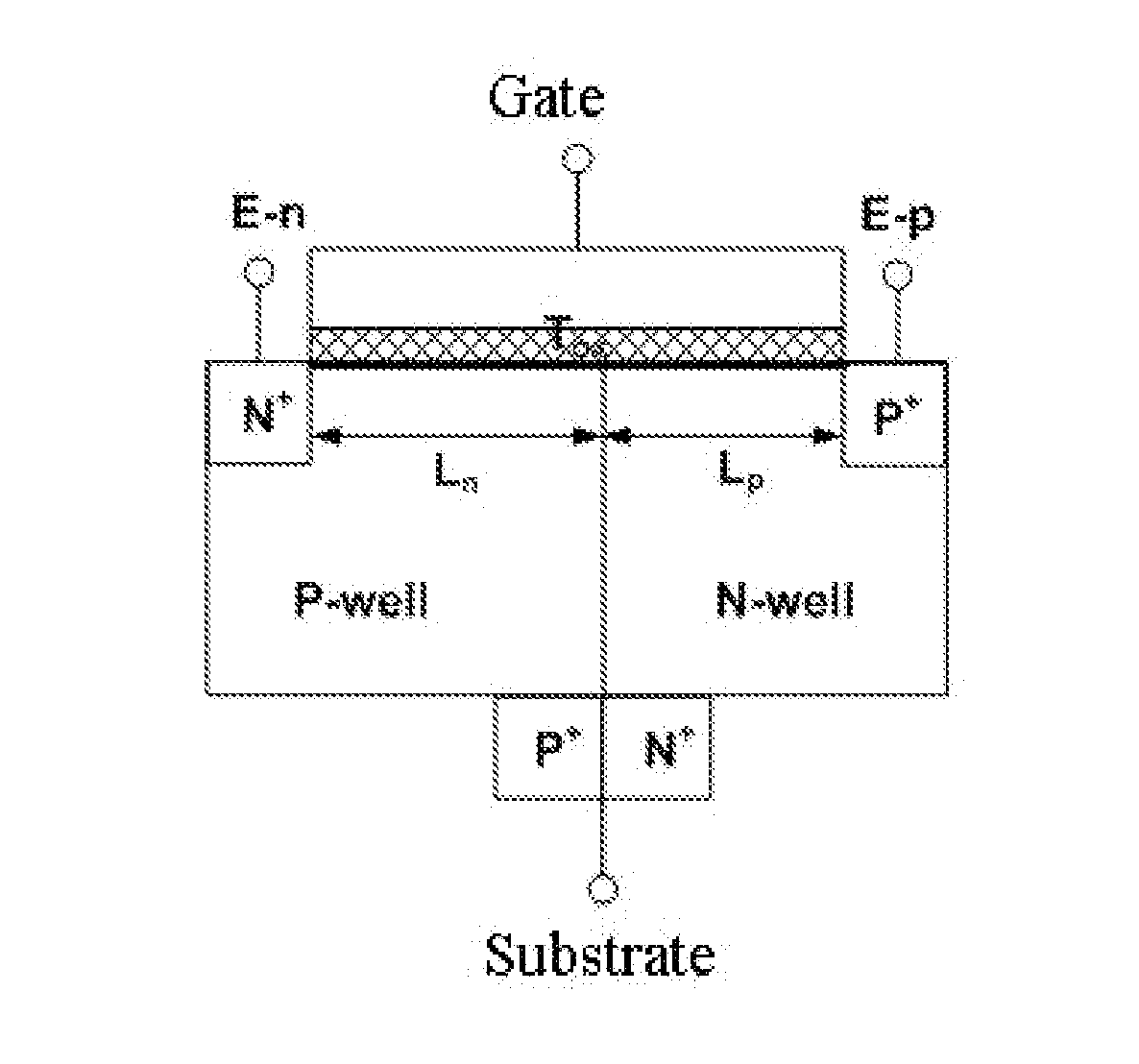
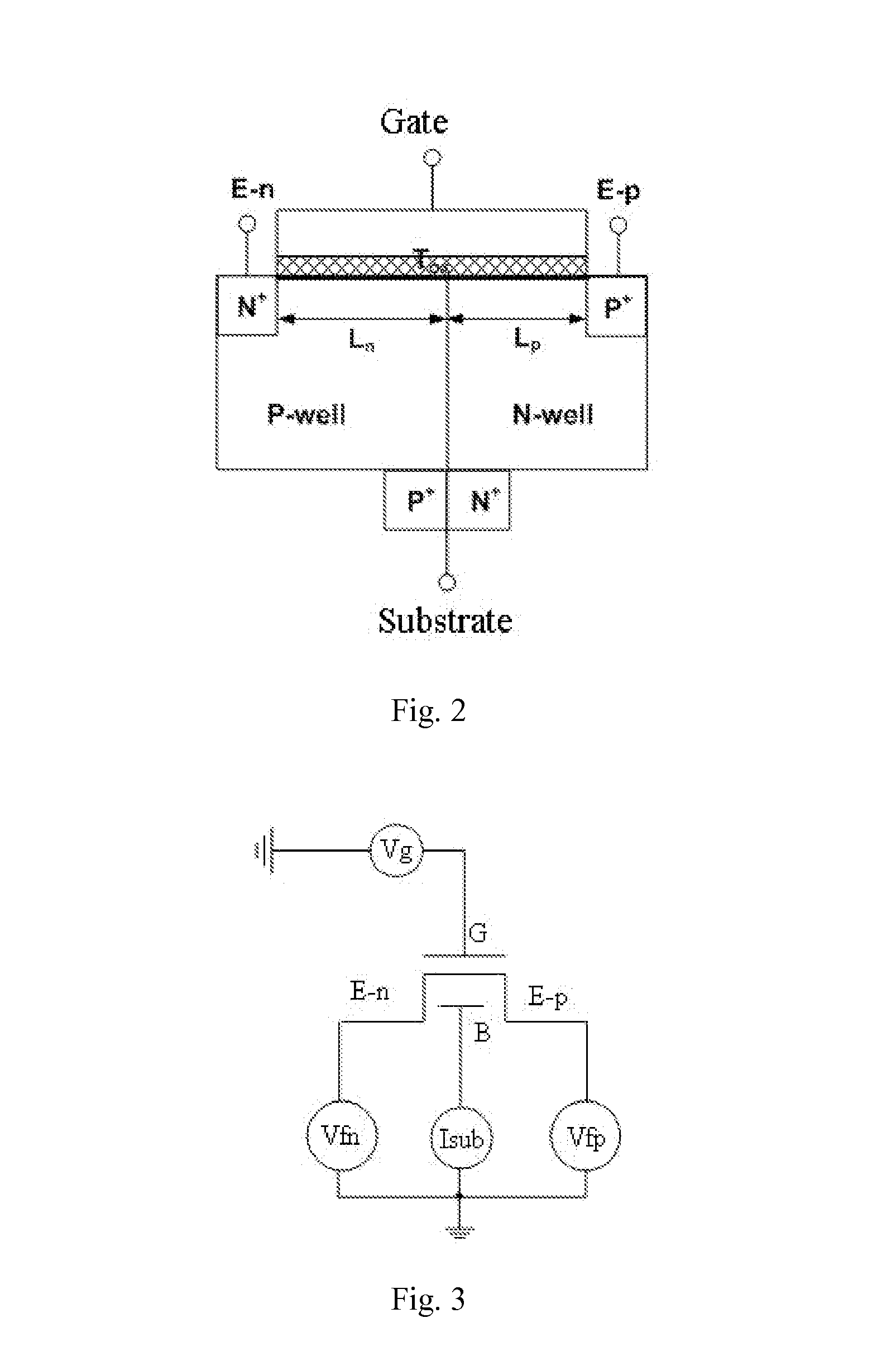
[0024]Hereinafter the present invention will be described in details in combination with the accompanying drawings and the preferred embodiments. The embodiments below are illustrated for explaining the present invention only but not limiting the scope thereof.

[0025]The objective of the present invention is to provide a testing structure and method capable of measuring the interface trap density of gate oxide for both n-type and p-type MOS devices at the same time, which proposes a method of the interface trap density of gate oxide for n-type and p-type MOS devices to be conducted in the same testing structure. This may not only shorten the measurement period by half but also decrease the costs for testing instruments used in the conventional method, because the present testing method is based on a simple current-voltage scanning test without the use of equipments such as pulse generator. The testing results obtained according to the present invention are featured with spectral peak...


PUM


Abstract

The present invention discloses a testing structure and method for interface trap density of gate oxide, relating to the field of quality and reliability researches of MOS devices. The present invention makes the interface traps density tests for gate oxide layers of n-type and p-type MOS devices completed on a same testing structure, this does not only shorten the measurement period by half but also decrease the costs for testing instruments, because the present testing method is based on a simple current-voltage scanning test without using equipments such as pulse generator required in conventional method. The testing results obtained according to the present invention are featured with spectral peak, which facilitates the data analysis and computation.

Description

FIELD OF THE INVENTION[0001]The present invention relates to the field of quality and reliability researches of MOS devices, in particular to a testing structure and method for interface trap density of gate oxide.BACKGROUND ART[0002]With rapid development of semiconductor technology and substantial improvement of microelectronic chip integration level, the design and process for integrated circuit has entered a nano-scale era. The gate oxide, as a core of a MOS device, plays a pivotal role in the assessment of quality and reliability of the MOS devices. The generation of interface traps of the gate oxide layer decreases mobility of the device and degrades performance of the device. Therefore, it's necessary to monitor the interface traps of the gate oxide layer during the process flows. Commonly used testing structure for interface trap density of gate oxide measurement is an oxide capacitance structure or a MOSFET device, which is shown in FIG. 1a as a 2-terminal capacitor element...

Claims


Application Information

Patent Timeline
IPC IPC(8): G01R31/26
CPCG01R31/2621H01L22/14H01L22/34H01L2924/0002
Inventor HE, YANDONGZHANG, GANGGANGLIU, XIAOYANZHANG, XING
Owner PEKING UNIV
Why Eureka
Try Eureka