IGBT with fast reverse recovery time rectifier and manufacturing method thereof

Inactive Publication Date: 2011-04-07
ANPEC ELECTRONICS CORPORATION
View PDF27 Cites 11 Cited by
  • Summary
  • Abstract
  • Description
  • Claims
  • Application Information

AI Technical Summary

Benefits of technology

[0011]In the present invention, a doped base region having a first conductivity type is formed in the doped region having a second conductivity type, wherein the doped region is located on any side of each gate insulating layer, so that the doped base region between two adjacent gate electrodes is divided into two doped base regions. Accordingly, the PN junction area of the bottom of the doped base region and the doped region is decreased to reduce the required reverse recovery time and to accelerate the swi

Problems solved by technology

However, the structure, which includes IGBT connected to an external diode, has higher production cost, more complicated packaging, and is large in size, so it does not conform to a trend of high degree of precision for electronic components.
Accordingly, reverse recovery time is required, so that the s

Method used


Image

  • IGBT with fast reverse recovery time rectifier and manufacturing method thereof
  • IGBT with fast reverse recovery time rectifier and manufacturing method thereof
  • IGBT with fast reverse recovery time rectifier and manufacturing method thereof

Examples


Example

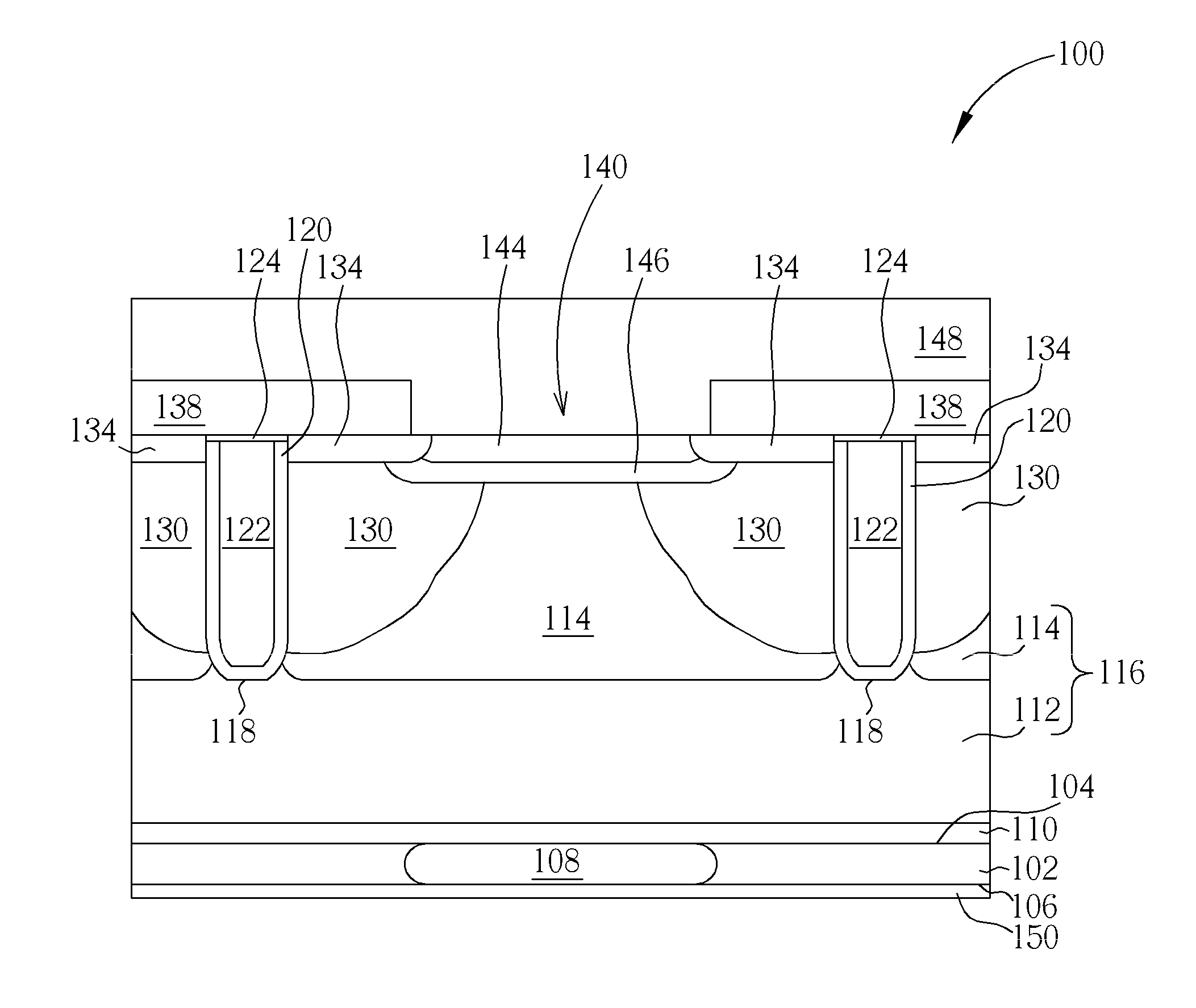
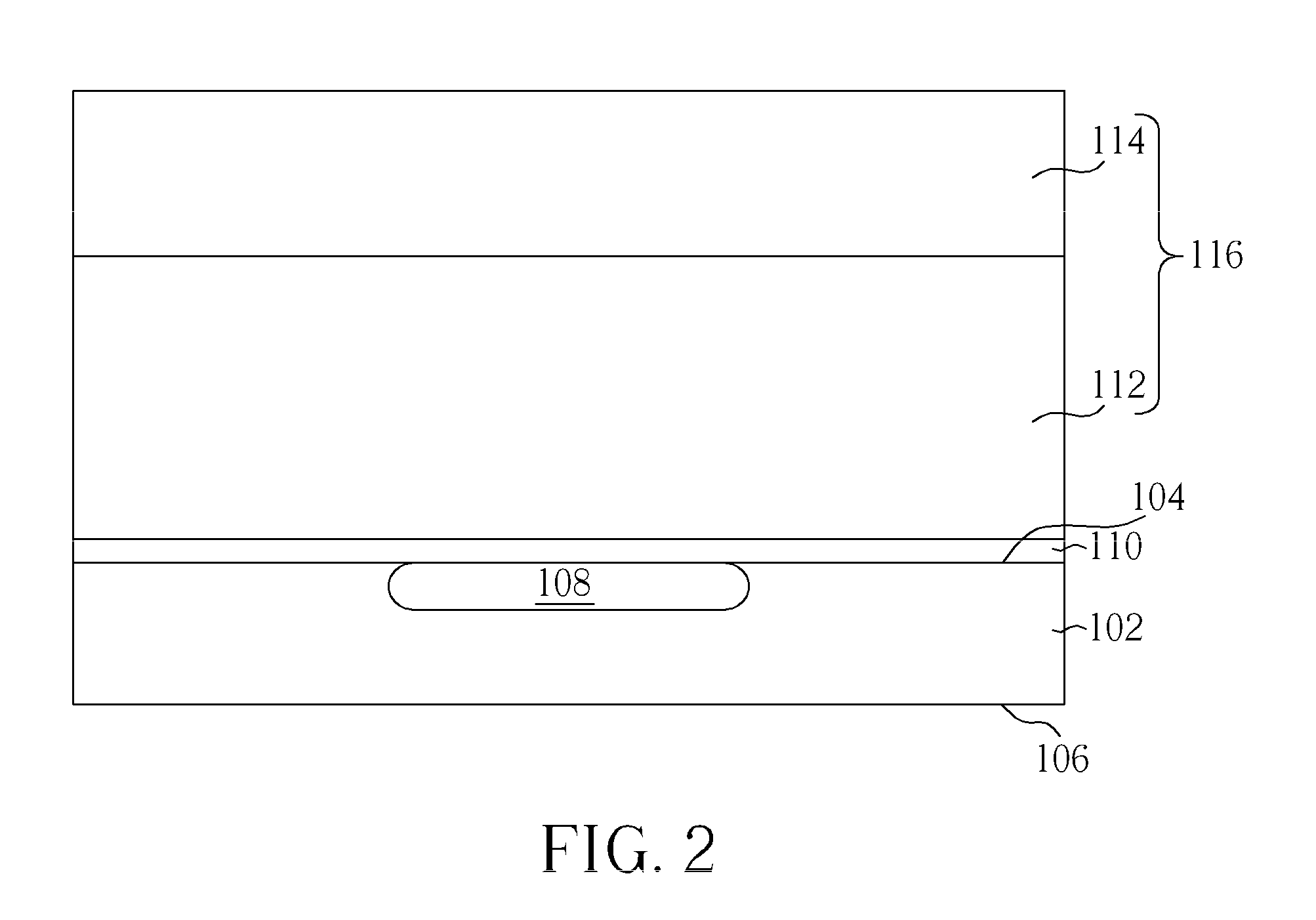
[0016]Please refer to FIGS. 2-7. FIGS. 2-7 are schematic diagrams illustrating a method of manufacturing an IGBT with a fast reverse recovery time rectifier according to a first embodiment of the present invention. As shown in FIG. 2, a semiconductor substrate 102 having a first conductivity type, such as a heavily doped P-type semiconductor substrate, is provided first, and the semiconductor substrate 102 includes an upper surface 104 and a lower surface 106. At least a doped cathode region 108 having a second conductivity type is doped in the semiconductor substrate 102, such as an N-type doped cathode region. In addition, a buffer layer 110 is disposed on the upper surface of the semiconductor substrate 102 of the present embodiment, and an epitaxial layer 112 is disposed on the buffer layer 110, wherein the buffer layer 110 and the epitaxial layer 112 have the second conductivity type, such as N-type. The first conductivity type of the present invention is not limited to P-type,...


PUM


Abstract

An IGBT with a fast reverse recovery time rectifier includes an N-type drift epitaxial layer, a gate, a gate insulating layer, a P-type doped base region, an N-type doped source region, a P-type doped contact region, and a P-type lightly doped region. The P-type doped base region is disposed in the N-type drift epitaxial layer, and the P-type doped contact region is disposed in the N-type drift epitaxial layer. The P-type lightly doped region is disposed between the P-type contact doped region and the N-type drift epitaxial layer, and is in contact with the N-type drift epitaxial layer.

Description

BACKGROUND OF THE INVENTION[0001]1. Field of the Invention[0002]This present invention is related to an insulated gate bipolar transistor (IGBT) with a fast reverse recovery time rectifier having and a manufacturing method thereof, and more particularly, to an IGBT with a rectifier having fast reverse recovery time for speeding up the reverse recovery of the rectifier and a manufacturing method thereof.[0003]2. Description of the Prior Art[0004]An IGBT is regarded as a composite structure combining a metal-oxide-semiconductor field effect transistor (MOSFET) and a bipolar junction transistor (BJT). By combining the MOSFET's characteristic of easy control with a gate electrode and the BJT's characteristic of low turn-on voltage drop, the IGBT is widely applied in high voltage and high power applications.[0005]Please refer to FIG. 1. FIG. 1 is a cross-sectional diagram illustrating a conventional IGBT. As shown in FIG. 1, the conventional IGBT 10 is described as follows. First, an N-t...

Claims


Application Information

Patent Timeline
IPC IPC(8): H01L29/739H01L21/331
CPCH01L29/0834H01L29/7397H01L29/66348H01L29/1095
Inventor LIN, WEI-CHIEHYEH, JEN-HAOCHEN, HO-TAI
Owner ANPEC ELECTRONICS CORPORATION
Why Eureka
Try Eureka