Method and apparatus for monitoring the position of a semiconductor processing robot
a semiconductor processing robot and position monitoring technology, applied in the field of robots, can solve the problems of blade position drift, blade may not arrive in the position expected, and the inability to accurately position the blade b>710/b> may be compromised
- Summary
- Abstract
- Description
- Claims
- Application Information
AI Technical Summary
Benefits of technology
Problems solved by technology
Method used
Image
Examples
Embodiment Construction
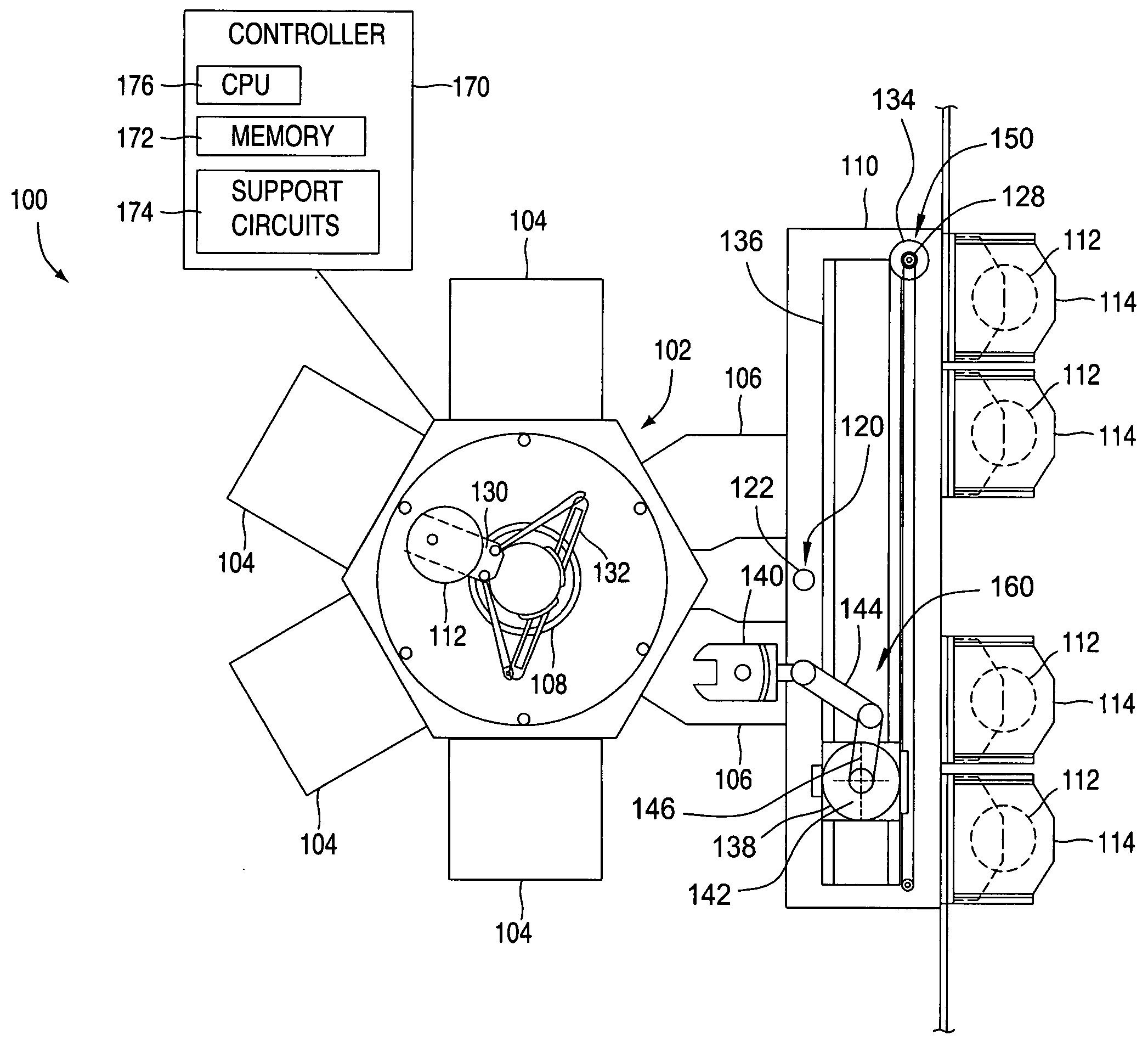
[0019]FIG. 1 depicts one embodiment of a semiconductor processing system 100 having at least one robotic positioning system 150. The exemplary processing system 100 generally includes a transfer chamber 102 circumscribed by one or more processing chambers 104, a factory interface 110 and one or more load lock chambers 106. The load lock chambers 106 are generally disposed between the transfer chamber 102 and the factory interface 110 to facilitate substrate transfer between a vacuum environment maintained in the transfer chamber 102 and a substantially ambient environment maintained in the factory interface 110.
[0020] The transfer chamber 102 defines an evacuable interior volume 116 through which substrates are transferred between the process chambers 104 coupled to the exterior of the transfer chamber 102. The process chambers 104 are typically bolted to the exterior of the transfer chamber 102. Examples of process chambers 104 that may be utilized include etch chambers, physical ...
PUM
 Abstract
Description
Claims
Application Information


