Metering-level 3D super-depth-of-field microscopy system and detection method

An ultra-depth-of-field microscopy and metrology-level technology, which is applied in the direction of measuring devices, optical testing flaws/defects, instruments, etc., can solve the problems of decreased detection accuracy of light-colored samples, failure to display the true microscopic color of materials, and inability to implement effective detection, etc.

Pending Publication Date: 2020-06-09
阳宇春 +1
View PDF0 Cites 10 Cited by
  • Summary
  • Abstract
  • Description
  • Claims
  • Application Information

AI Technical Summary

Problems solved by technology

[0005] Laser confocal microscopy technology: This method uses the principle of laser and pinhole confocal imaging to scan the sample surface, obtain the microscopic topography point cloud data of the sample surface, and then perform three-dimensional modeling, which can realize the z-axis nanoscale detection accuracy , with high 3D high-precision measurement; however, this type of instrument has the following technical problems: the price is too expensive, and it is only suitable for a very small number of users. Through this method, only grayscale images and black and white 3D models can be obtained, and there is no display material Microscopic real color, its large-area 3D image acquisition is based on the principle of splicing multiple 3D images into a super-large 3D model. The algorithm itself will introduce new errors, resulting in a decrease in accuracy, so it is more suitable for small-scale observations
However, in the process of realizing the embodiment of the present invention, the inventors of the present application found that the above-mentioned 3D ultra-depth-of-field microscopy technology is limited in that: the optical microscope is limited by the illumination mode, the field curvature of the optical lens, distortion, algorithm and the optical depth-of-field algorithm, and the image has certain limitations. Distortion; and this type of instrument cannot effectively detect smooth surfaces (such as mirrors or ceramics) and transparent samples (such as glass), and the detection accuracy of light-colored samples with low contrast is significantly reduced; and large-area 3D image acquisition is required. The principle of splicing multiple 3D models into a super-large 3D model will introduce new errors into the algorithm itself, which will cause its detection accuracy to fail to meet the growing detection needs; therefore, in view of the above technical problems, it is urgent to research and design a metrology-level The 3D ultra-depth-of-field microscope system and detection method meet the requirements of relatively low cost. It is a microscope system that can detect 3D micro-nano dimensions in a large area and can reflect the real details and real colors of the sample. It can comprehensively observe the target and meet the requirements of increasingly complex fine Testing requirements

Method used


Image

  • Metering-level 3D super-depth-of-field microscopy system and detection method
  • Metering-level 3D super-depth-of-field microscopy system and detection method
  • Metering-level 3D super-depth-of-field microscopy system and detection method

Examples


Embodiment 1

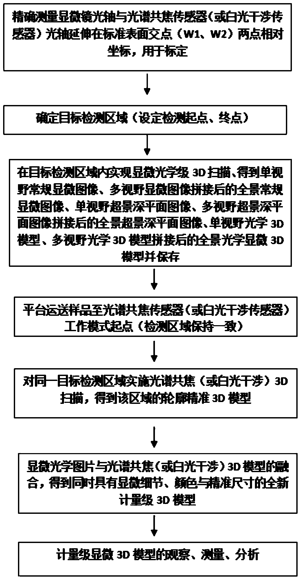
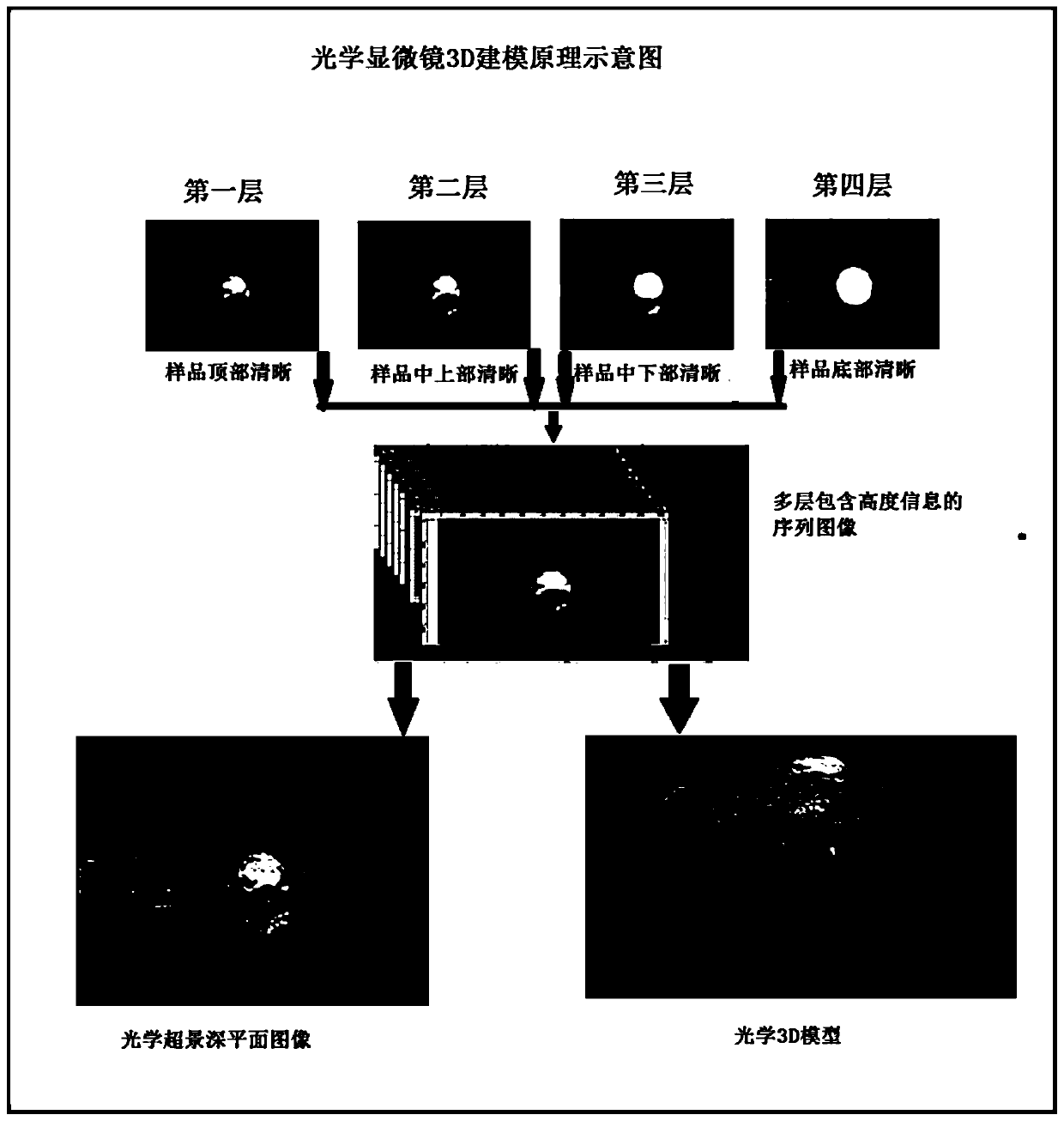
[0074] The embodiment is basically like Figure 1 to Figure 5 Shown: This embodiment provides a metrology-level 3D ultra-depth-of-field microscopy detection method, which runs in a metrological-level 3D ultra-depth-of-field microscopy system, which includes an optical microscope 1, a spectral confocal sensor 2 or white light interference sensor, xyz axis electric displacement platform 3 and corresponding control module and PC processor 8; wherein the control module is connected to PC processor 8, and the control module includes an xyz electric control unit connected to xyz axis electric displacement platform 3 71. The spectral confocal processor 72 connected to the spectral confocal sensor 2 or the white light interference signal processor and the power supply module connected to the white light interference sensor; this embodiment provides the spectral confocal sensor 2 and the spectral confocal processor 72 as For example, the xyz-axis electric displacement platform 3 include...

Embodiment 2

[0133] This embodiment is basically the same as embodiment 1, and the difference is that: this embodiment takes the optical detection sensor as an example of a white light interference sensor, and compares the 3D point cloud model obtained by the white light interference sensor with the single-field superstructure obtained by the optical microscope 1. Take the depth-of-field plane image fusion process B as an example. The specific fusion method includes the following steps:

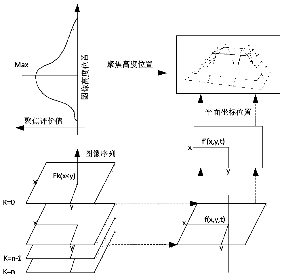
[0134] (1) Fix the xy-axis coordinate position of the xyz-axis electric displacement platform 3, adjust the height of the optical microscope 1z-axis, and reconstruct the single-field super-depth map of the object at this position; calculate the xy corresponding to each point of the image pixel on the single-field super-field map Actual coordinate position;

[0135] (2) The single-field super-depth-of-field picture is a rectangle. According to the size of the microscopic field of view, two diagonal corners of t...

Embodiment 3

[0137] Embodiment 3 is basically the same as embodiment 1, and the difference is that: this embodiment uses the xyz axis data of the 3D point cloud model obtained by the spectral confocal sensor 2 to replace the xyz axis data of the corresponding area optical microscope 3D model as an example. The fusion method includes the following steps:

[0138] (1) Perform step 1, step 2, step 3, and step 4 in the process of embodiment 1;

[0139] (2) Through the above process, the optical microscope 3D model and the spectral confocal sensor 2 scanning 3D model can be directly obtained. The optical microscope 3D model and the spectral confocal sensor 2 scanning model have the same starting point and ending point in the xy direction, and directly extract the spectrum. The confocal sensor 2 scans all data on the xyz axis of the model, and the xyz direction data is imported into the three-dimensional coordinates of the optical microscope 3D model to generate a new model, which is based on the mod...


PUM


Abstract

The invention discloses a metering-level 3D super-depth-of-field microscopy system and a detection method, and relates to the technical field of photoelectric nondestructive 3D detection. The microscopic system comprises an optical microscope, a spectral confocal sensor or a white light interference sensor, an xyz-axis electric displacement platform, a control module and a PC processor. The xyz-axis electric displacement platform comprises an xy-axis translation platform and a z-axis lifting module; the optical microscope is provided with an illumination light source and an image acquisition unit, the control module comprises an xyz electric control unit, a processor connected with the spectral confocal sensor or the white light interference sensor and a power supply module, and the imageacquisition unit is used for acquiring image information of a target detection area and transmitting the image information to the PC processor; by implementing the technical scheme, a sample can be observed in a nondestructive manner, photographing, 3D true color imaging and 3D accurate measurement can be performed on the microscopic state of the surface of a material in an ultra-large area, the measurement-level detection precision is realized, the details and the real color of the microscopic sample are kept, and the method has a good application prospect.

Description

Technical field [0001] The present invention relates to the technical field of photoelectric non-destructive 3D detection, and more specifically, to a metrology-level 3D ultra-depth-of-field microscopy system and detection method. Background technique [0002] Non-contact 3D surface detection technology describes the use of non-destructive optical technology to capture the 3D space coordinates of points on the surface of the object on natural or processed surfaces to achieve the measurement and characterization of micron or nano-scale features; and contact surface detection technology Compared with the optical inspection system, it has major advantages. It will not damage the object to be measured and can measure through transparent media. Therefore, the application field has achieved rapid development and is widely used in MEMS, semiconductors, nanomaterials, biomedicine, and industrial detection. The most common optical detection technologies include spectroscopic confocal prof...

Claims


Application Information

Patent Timeline
Patent Type & Authority Applications(China)
IPC IPC(8): G01B11/24G01N21/95
CPCG01B11/24G01B11/2441G01N21/95
Inventor 阳宇春孙亮
Owner 阳宇春
Why Eureka
Try Eureka