
A real-time monitoring optical path system for micro-nano structure morphology in inkjet printing

A technology of inkjet printing and real-time monitoring, applied in measurement devices, optical devices, instruments, etc., can solve the problems of reducing printing efficiency, inability to conduct real-time analysis and observation, etc., to achieve convenient and adjustable components, real-time, The effect of low environment dependence

Active Publication Date: 2022-06-28
QINGDAO UNIV OF SCI & TECH
View PDF8 Cites 0 Cited by
  • Summary
  • Abstract
  • Description
  • Claims
  • Application Information

AI Technical Summary

Problems solved by technology

Although these solutions are real-time sampling, they cannot be analyzed and observed in real time. It is necessary to analyze the printing results after printing and compare them with the printing parameters. This not only reduces the printing efficiency to a certain extent, but also makes it difficult to find errors during the printing Defects are corrected in a timely manner

Method used


Image

  • A real-time monitoring optical path system for micro-nano structure morphology in inkjet printing
  • A real-time monitoring optical path system for micro-nano structure morphology in inkjet printing
  • A real-time monitoring optical path system for micro-nano structure morphology in inkjet printing

Examples


Embodiment

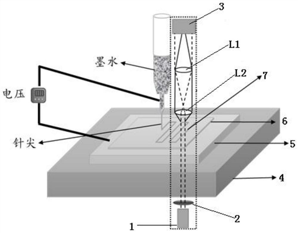
[0017] The main structure of the optical path system for real-time monitoring of micro-nano structure morphology in inkjet printing described in this embodiment is as follows: figure 1 As shown, including laser 1, attenuator 2, first convex lens L1, second convex lens L2 and CCD camera 3, the center of each optical element is located on a straight line, and the surface is perpendicular to the beam propagation direction to ensure uniform beam propagation; printing The distance between the sample and the first convex lens L1 and the focal length f of the first convex lens L1 1 Equal, the distance between the second convex lens L2 and the CCD camera 3 is the same as the focal length f of the second convex lens L2 2 equal, the distance between the first convex lens L1 and the second convex lens L2 is the sum of the focal lengths of the two to ensure that the resulting image is a clear image; the beam emitted by the laser 1 is adjusted by the attenuator 3 to adjust the beam energy,...


PUM


Abstract

The invention belongs to the technical field of printed electronics, and relates to an optical path system for real-time monitoring of micro-nano structure morphology in inkjet printing. The beam emitted by the laser passes through an attenuator to adjust the energy of the beam. Convex lens, the light finally converges on the CCD camera, and the CCD camera is connected to an external computer. The printed structure on the printed sample can be observed in real time through the computer. According to the focal length of the selected convex lens, the result observed by the computer is a scaled image of the printed structure. ; The optical path is simple and intuitive, the components are convenient and adjustable, the principle is reliable, the operation is convenient, and it is easy to implement. It can be widely used in various micro-nano structures and electronic manufacturing fields based on inkjet printing technology.

Description

Technical field: [0001] The invention belongs to the technical field of printing electronics, and relates to a real-time monitoring system for inkjet printing, in particular to a real-time monitoring optical path system for micro-nano structure morphology in inkjet printing. Background technique: [0002] Inkjet printing technology (InkjetPrinting) is a kind of "direct write" printed electronic technology, which uses gas pressure, electric field force or other forms of force to spray the functional oil film drop by drop on the surface of various substrates under the precise control of the computer. , to obtain specific micro-nano structures or thin films. This technology has the advantages of low cost, environmental friendliness, high efficiency and direct writing, and has been widely used in the field of new electronic materials in recent years. According to the different ways of inkjet printing, inkjet printing can be divided into two types: continuous inkjet printing (the...

Claims


Application Information

Patent Timeline
Patent Type & Authority Patents(China)
IPC IPC(8): G01B11/30
Inventor 吕浩秦汉唐张校
Owner QINGDAO UNIV OF SCI & TECH
Learn More