Plasma display panel

a technology of display panels and plasma, which is applied in the direction of address electrodes, static indicating devices, instruments, etc., can solve the problems of affecting the performance of the exhaust system, and wasting too much time for the address period, so as to reduce the delay of discharge and improve the exhaust performance

Inactive Publication Date: 2005-05-12
PANASONIC CORP
View PDF12 Cites 10 Cited by
  • Summary
  • Abstract
  • Description
  • Claims
  • Application Information

AI Technical Summary

Benefits of technology

[0012] With this structure, discharge cells are divided into a first discharge space, which is a main discharge cell for displaying image data, and a second discharge space, which is a priming discharge cell. And the main discharge cell is stably supplied with priming particles generated inside the priming discharge cell through the clearance so as to reduce a discharge delay. It also becomes possible to improve exhaust performance in the discharge cells.

Problems solved by technology

In this type of PDP, a large delay in discharge occurs during the address period, thereby making the address operation unstable, or completion of the address operation requires a long address time, thereby spending too much time for the address period.
However, in these conventional PDPs, when the number of discharge cells is increased as a result of achieved higher definition, more time must be spent for the address time and less time must be spent for the sustain period, thereby making it difficult to achieve high brightness or high gradation.
Furthermore, since the address properties are greatly affected by the address process, it is demanded to reduce a discharge delay during the addressing, thereby accelerating the address time.
In spite of this demand, in conventional PDPs performing a priming discharge in the front plate surface, a discharge delay during the addressing cannot be reduced sufficiently; the operating margin of an auxiliary discharge is small; and a false discharge is induced to make the operation unstable.
Moreover, since the auxiliary discharge is performed in the front plate surface, more priming particles than necessary for priming are applied to an adjacent discharge cell, thereby causing crosstalk.

Method used


Image

  • Plasma display panel
  • Plasma display panel
  • Plasma display panel

Examples


first exemplary embodiment

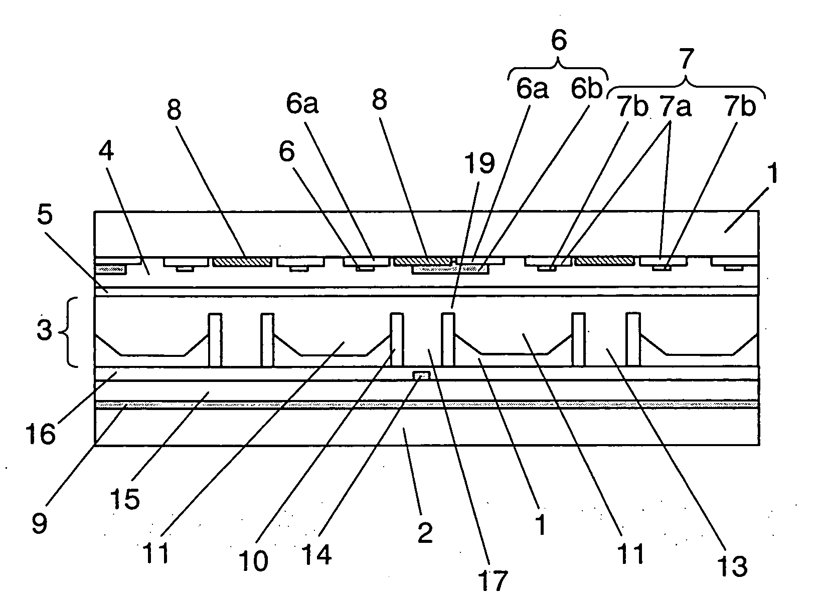
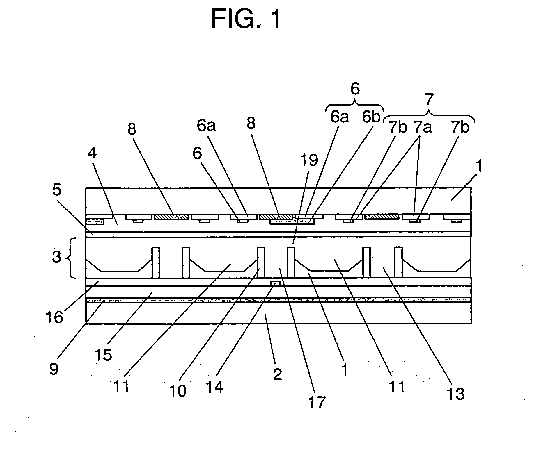
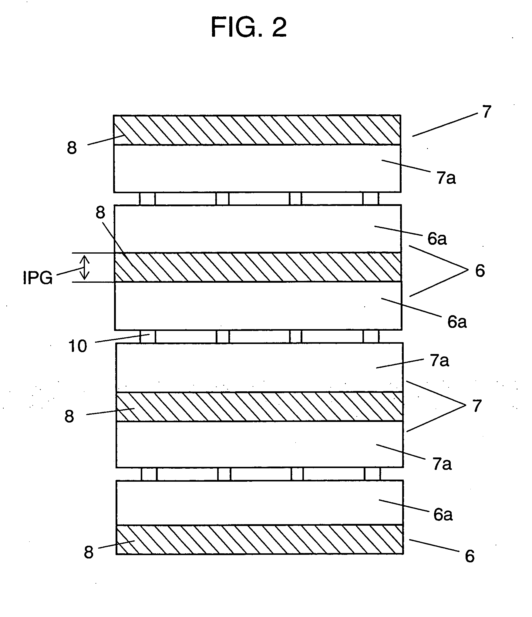
[0024]FIG. 1 is a cross sectional view of a PDP according to a first embodiment of the present invention, and FIG. 2 is a schematic plan view showing an electrode arrangement on a front substrate side, which is a first substrate side of the PDP according to the first embodiment of the present invention. FIG. 3 is a schematic perspective view showing a back substrate side, which is a second substrate side of the PDP according to the first embodiment of the present invention.

[0025] As shown in FIG. 1, the PDP according to the present invention includes front substrate 1 which is a first substrate made of glass, and back substrate 2 which is a second substrate made of glass disposed to face each other with discharge space 3 therebetween, and discharge space 3 is sealed with neon, xenon and the like as gasses for irradiating ultraviolet rays by discharge. On front substrate 1, a group of belt-shaped electrodes consisting of pairs of scan electrodes 6 as first electrodes and sustain ele...

second exemplary embodiment

[0039]FIG. 6 is a cross sectional view of a PDP according to a second embodiment of the present invention, and a clearance is provided by reducing a thickness of dielectric layer 4 on front substrate 1. To be more specific, dielectric layer 4 on front substrate 1 is made thinner in a portion corresponding to the barrier ribs which form priming discharge cells 17 by applying a convex patterning onto front substrate 1 side, thereby forming priming slit 20 as the clearance. Thus, priming particles can be stably supplied to at least adjacent main discharge cells 11.

[0040]FIG. 7 shows a relation between a clearance gap and the amount of crosstalk. In FIG. 7, the horizontal axis indicates a clearance gap in the unit μm, and the vertical axis indicates a wall voltage (the unit V) reduced by crosstalk between adjacent main discharge cells. Since the wall voltage decreases with increasing crosstalk amount, the vertical axis indicates crosstalk amount. A parameter, IPG stands for Inter Pixel...

third exemplary embodiment

[0041]FIG. 8 shows a statistical delay time in discharge with respect to voltage Vpr to be applied to priming electrodes 14 in the case of cells corresponding to scan electrode Yn and cells corresponding to scan electrode Yn+1 which are respectively the n-th and n+1th of scan electrodes 6. When a scan pulse is applied to scan electrode Yn or the n-th of scan electrodes 6, a discharge delay in the n-th cells is rather large because a priming discharge is being performed; however, a discharge delay is decreased by increasing priming voltage Vpr. Since the n+1th discharge cells have been already affected by a priming discharge, a discharge delay is extremely small.

[0042]FIG. 9 is a cross sectional view of a PDP in a case that in priming discharge cells 17, there is a size difference between clearance 23 above lateral rib part 22 of main discharge cells 21 corresponding to scan electrode Yn or the n-th of scan electrodes 6 and clearance 26 above lateral rib part 25 of main discharge ce...


PUM


Abstract

A plasma display panel can reduce a discharge delay in address discharge, thereby performing high-speed addressing in a stable manner. A front substrate (1) and a back substrate (2) are disposed to face each other, and a discharge space (3) is formed and partitioned by barrier ribs (10) so as to form priming discharge cells (17) and main discharge cells (11). A clearance (19) is provided between the barrier ribs (10) of the priming discharge cells (17) and the front substrate (1), and priming particles generated in the priming discharge cells (17) are supplied to the main discharge cells (11) through the clearance (19), whereby a PDP performing high-speed addressing is obtained.

Description

TECHNICAL FIELD [0001] The present invention relates to plasma display panels used for wall-hung TVs and large-size monitors. BACKGROUND ART [0002] An AC surface discharge type plasma display panel (hereinafter referred to as PDP), which is a typical AC type PDP, is formed of a front plate made of a glass substrate having scan electrodes and sustain electrodes provided thereon for a surface discharge, and a back plate made of a glass substrate having data electrodes provided thereon. The front plate and the back plate are disposed to face each other in parallel in such a manner that the electrodes on both plates form a matrix, and that a discharge space is formed between the plates. And the outer part of the plates thus combined is sealed with a sealing member such as a glass frit. Between the substrates, discharge cells partitioned by barrier ribs are formed, and phosphor layers are provided in the cell spaces formed by the barrier ribs. In a PDP with this structure, ultraviolet ra...

Claims


Application Information

Patent Timeline
Patent Type & Authority Applications(United States)
IPC IPC(8): H01J11/12H01J11/14H01J11/22H01J11/24H01J11/26H01J11/28H01J11/34H01J11/36H01J11/38
CPCH01J11/12H01J11/24H01J2211/361H01J11/38H01J11/36H01J11/22
Inventor TACHIBANA, HIROYUKIFUJITANI, MORIONISHIO, TSUYOSHIANDO, TORUMIZUNO, KOICHI
Owner PANASONIC CORP
Why Eureka
Try Eureka