Insulated gate field-effect transistor having III-VI source/drain layer(s)

a field-effect transistor and gate field-effect technology, which is applied in the field of fabrication of transistors, can solve the problems of reducing the efficacy of this approach, and the thickness control of interfacial layers or films of the types described in the above-cited patent application, and may not be easy to achiev

Inactive Publication Date: 2005-05-19
ACORN SEMI LLC
View PDF4 Cites 52 Cited by
  • Summary
  • Abstract
  • Description
  • Claims
  • Application Information

AI Technical Summary

Benefits of technology

[0021] In the above-cited U.S. patent applications Ser. Nos. 10 / 832,576 and 10 / 754,966, Grupp and Connelly describe an insulated gate field-effect transistor having passivated Schottky barriers to the channel, in which an “interface layer” is imposed between the channel material and the source / drain material of a FET. The interface layer is used to “depin” the Fermi level of the metal from deep within the gap of a semiconductor in the vicinity of the contact, reducing the Schottky barrier for a metal of an appropriate workfunction (relatively low for an n-channel FET, and relatively high for a p-channel FET). By depinning the Fermi level, the present inventors mean a condition wherein, to a substantial degree, dangling bonds that may otherwise be present at the semiconductor surface have been terminated, and the effects of a charge dipole associated with metal / semiconductor interactions have been overcome, or at least reduced, by displacing the semiconductor a sufficient distance from the metal.

Problems solved by technology

However, metal / semiconductor interactions reduce the efficacy of this approach.
Controlling the thickness of interfacial layers or films of the types described in the above-cited patent applications (e.g., materials which, in their bulk form, are insulators, such as silicon nitride, Si3N4, or oxides of semiconductors, such as SiO2, or of metals, such as ZrO2) may not be easy.

Method used


Image

  • Insulated gate field-effect transistor having III-VI source/drain layer(s)
  • Insulated gate field-effect transistor having III-VI source/drain layer(s)
  • Insulated gate field-effect transistor having III-VI source/drain layer(s)

Examples


Embodiment Construction

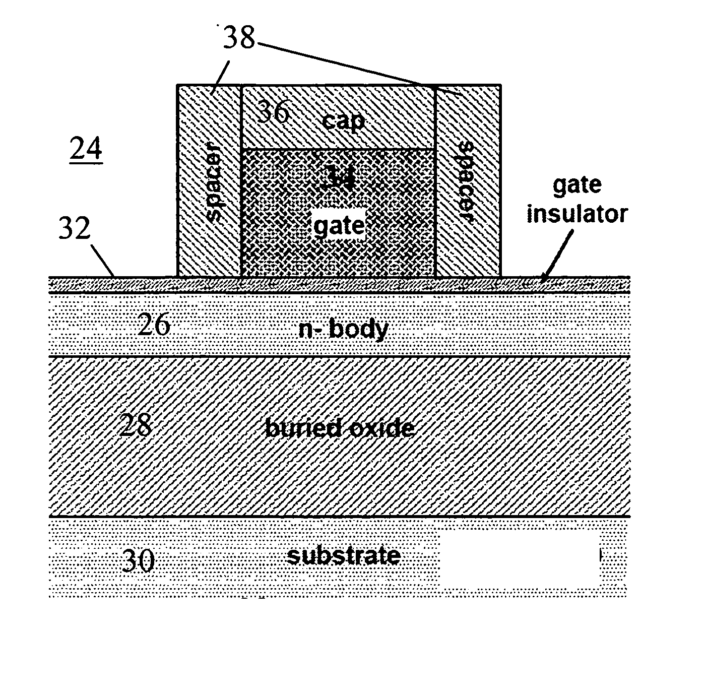
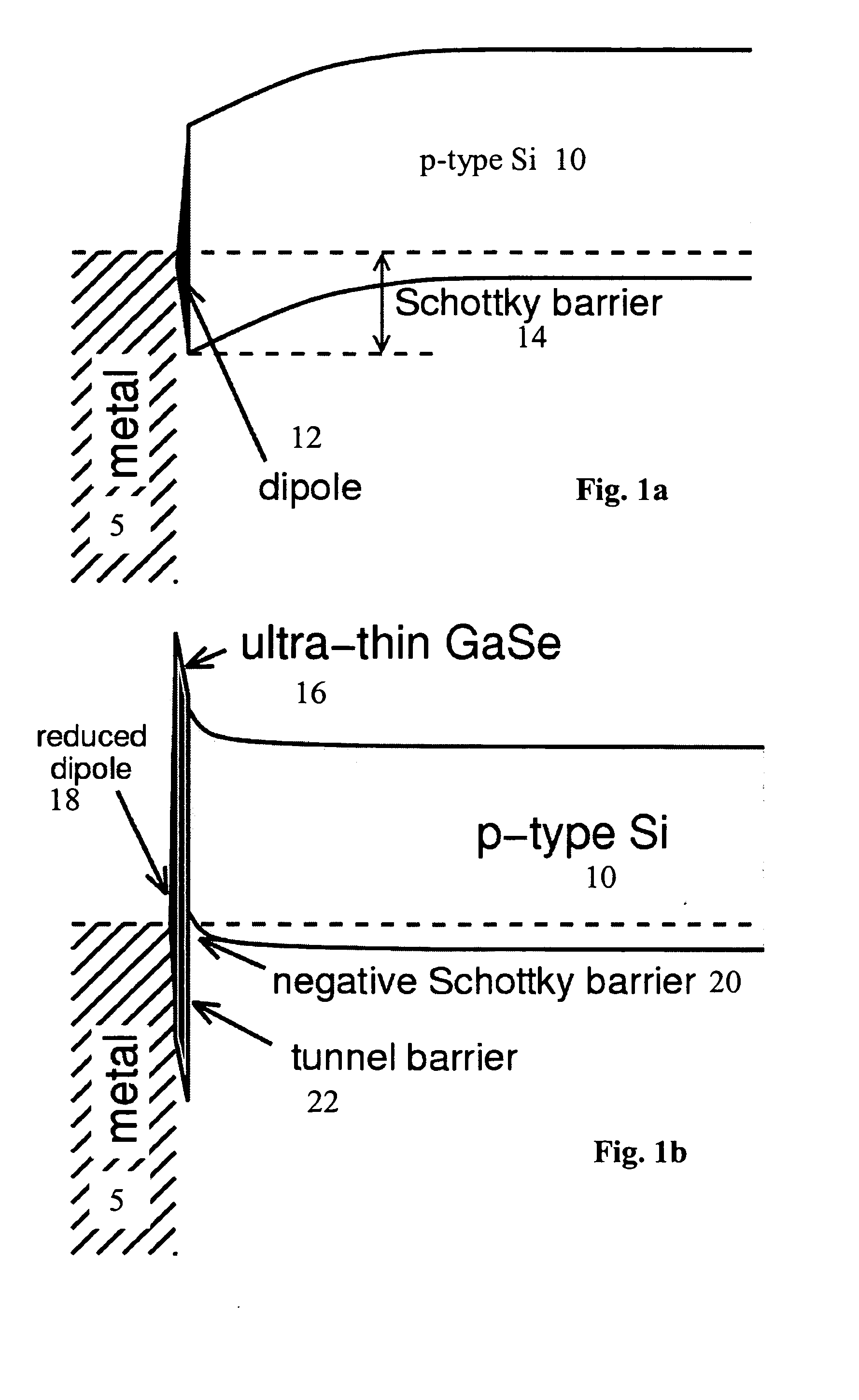
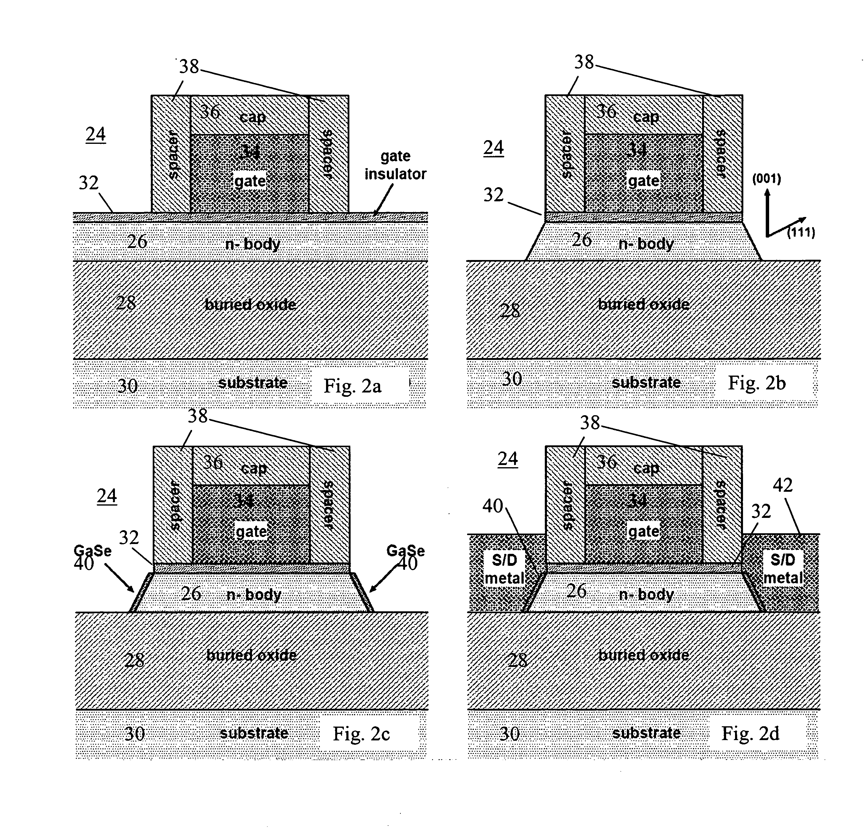
[0030] Described herein are various embodiments of the present invention, including a transistor having one or more channel taps (source(s) and / or drain(s)) containing a stack consisting at least in part of a semiconductor, an interfacial III-VI layered compound, for example GaSe; and a conductor, which may be metal. The III-VI compound may be formed on a {111} surface of the semiconductor, for example Si or an alloy of Si, forming the channel. It may be epitaxially formed as a bilayer, consisting of a single layer of element(s) from Groups IIIA-B, such as Ga, and a single layer of Group VI elements, such as Se. The {111} source and / or drain surface(s) may be of a separate plane than the channel plane, possibly exposed by a selective etch.

[0031] For purposes of the present invention, a III-VI compound includes one or more element(s) from Groups IIIA-B (e.g., B, Al, Sc, Ga, Y, In, La, Tl, Ac, and Uut) and one or more Group VIA elements (e.g., O, S, Se, Te, Po, Uuh) in approximately ...


PUM


Abstract

A transistor includes one or more channel taps containing a stack consisting at least in part of a semiconductor an interfacial III-VI layered compound and a conductor. The III-VI compound consists primarily of atoms from Groups IIIA-B and from Group VIA of the Periodic Table of the Elements in an approximate 1:1 ratio. These materials may be formed as layers of covalently bonded elements from Groups IIIA-B and covalently bonded Group VIA elements, adjacent and respective planes of which may be bonded by Van der Waals forces (e.g., to form a single bilayer consisting of a single plane of atoms from Groups IIIA-B and a single plane of Group VIA atoms). One particular III-VI material from which the interfacial layer is made, especially for p-channel transistors, is GaSe. Other III-VI compounds, whether pure compounds or alloys of pure compounds, may also be used.

Description

RELATED APPLICATIONS [0001] The present application is a continuation-in-part of the following co-pending U.S. patent applications: [0002] 1. Ser. No. 10 / 832,576, filed Apr. 26, 2004, entitled TRANSISTOR WITH WORKFUNCTION INDUCED CHARGE LAYER, which claims priority from U.S. Provisional Patent Application 60 / 535082, filed Jan. 7, 2004; [0003] 2. Ser. No. 10 / 217,758, filed Aug. 12, 2002, entitled METHOD FOR DEPINNING THE FERMI LEVEL OF A SEMICONDUCTOR AT AN ELECTRICAL JUNCTION AND DEVICES INCORPORATING SUCH JUNCTIONS; and [0004] 3. Ser. No. 10 / 754,966, filed Jan. 9, 2004, entitled INSULATED GATE FIELD EFFECT TRANSISTOR HAVING PASSIVATED SCHOTTKY BARRIERS TO THE CHANNEL, which is a divisional of co-pending U.S. patent application Ser. No. 10 / 342,576, filed Jan. 14, 2003, entitled INSULATED GATE FIELD EFFECT TRANSISTOR HAVING PASSIVATED SCHOTTKY BARRIERS TO THE CHANNEL, which is a continuation-in-part of co-pending U.S. patent application Ser. No. 10 / 217,758; all of which are assigned...

Claims


Application Information

Patent Timeline
Patent Type & Authority Applications(United States)
IPC IPC(8): H01L21/28H01L29/04H01L29/786H01L31/119
CPCH01L29/045H01L29/785H01L29/78684H01L29/78681H01L29/78654
Inventor FAULKNER, CARLCONNELLY, DANIEL J.GRUPP, DANIEL E.
Owner ACORN SEMI LLC
Why Eureka
Try Eureka