Solid-state imaging device and method of manufacturing solid-state imaging device background of the invention

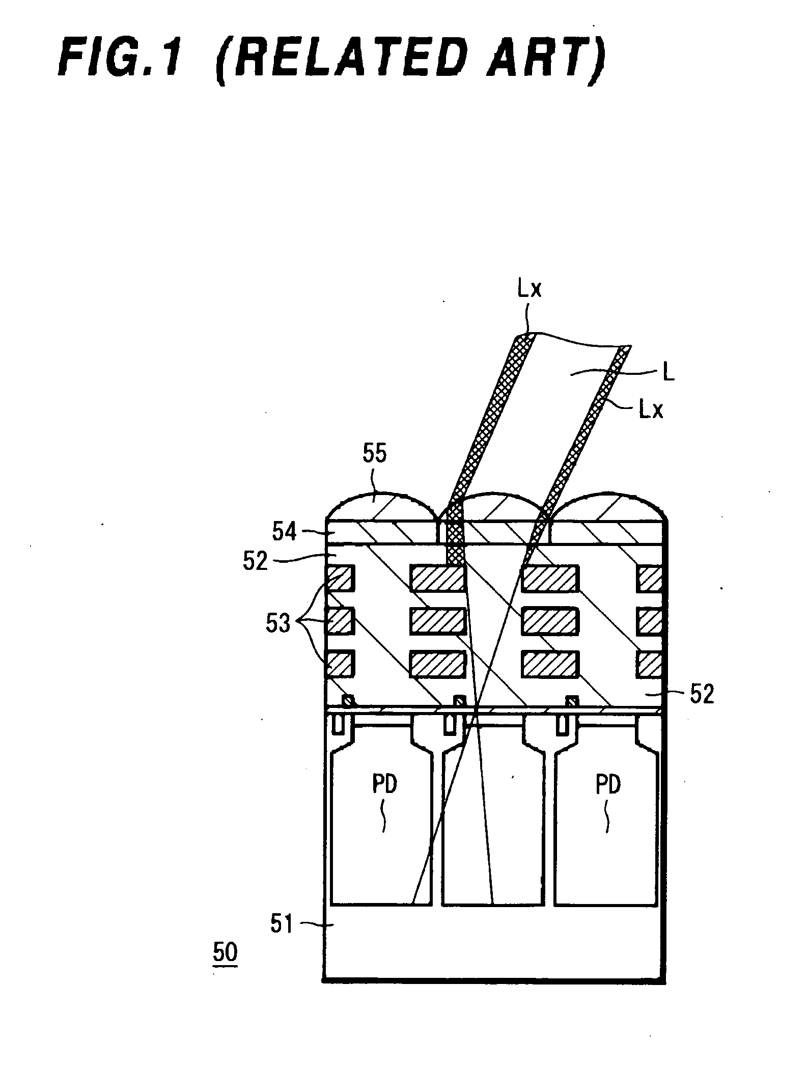
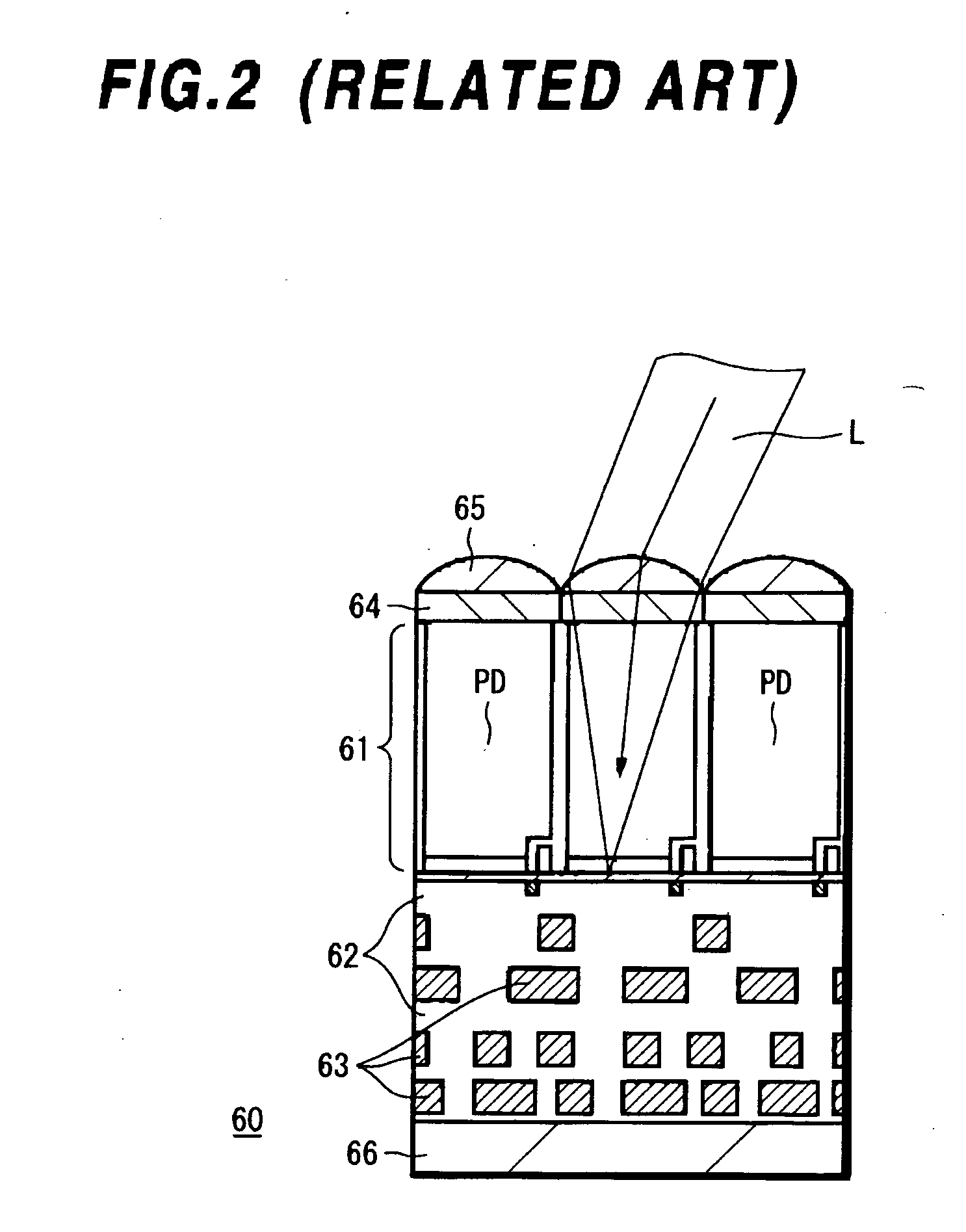
a solid-state imaging and imaging device technology, applied in the direction of solid-state devices, basic electric elements, radiation controlled devices, etc., can solve the problems of unavoidable increase in the distance between the lens b>55/b> and the photodiode pd of the light-receiving sensor portion, and is not possible to manufacture alignment marks, etc., to achieve effective vignetting factor and improve sensitivity

Inactive Publication Date: 2005-05-19
SONY CORP
View PDF1 Cites 144 Cited by
  • Summary
  • Abstract
  • Description
  • Claims
  • Application Information

AI Technical Summary

Benefits of technology

[0034] In view of the aforesaid aspect, it is an object of the present invention to provide a solid-state imaging device which can realize a back-illuminated type solid-state imaging device by forming an alignment mark for precisely aligning a photodiode of a light-receiving sensor portion and a lens and a pad contact to the back-illuminated type solid-state imaging device and a method of manufacturing a solid-state imaging device.

Problems solved by technology

However, as the solid-state imaging device is microminiaturized increasingly, the pitch of interconnection becomes narrower and the interconnection layer 53 is formed of much more layers so that a distance between the lens 55 and the photodiode PD of the light-receiving sensor portion is increased unavoidably.
However, in the structure of the back-illuminated type solid-state imaging device according to the related art, it has not been considered so far to form an alignment mark.
Also, in the back-illuminated type solid-state imaging device, since the lens is formed on the back side of the silicon substrate, it is not possible to manufacture the alignment mark of the lens relative to the photodiode by a method similar to the alignment mark producing method in the surface-illuminated type solid-state imaging device (method of forming the alignment mark on the surface of the silicon substrate).
Also, similarly, since the supporting substrate and the like are attached to the side of the interconnection layer, it is impossible to form a pad contact by an ordinary method.
Otherwise, it becomes impossible to realize a back-illuminated type solid-state imaging device, and hence it becomes difficult to microminiaturize the solid-state imaging device and to improve performance such as resolution.

Method used


Image

  • Solid-state imaging device and method of manufacturing solid-state imaging device background of the invention
  • Solid-state imaging device and method of manufacturing solid-state imaging device background of the invention
  • Solid-state imaging device and method of manufacturing solid-state imaging device background of the invention

Examples


Embodiment Construction

[0108] The present invention will now be described in detail with reference to the drawings.

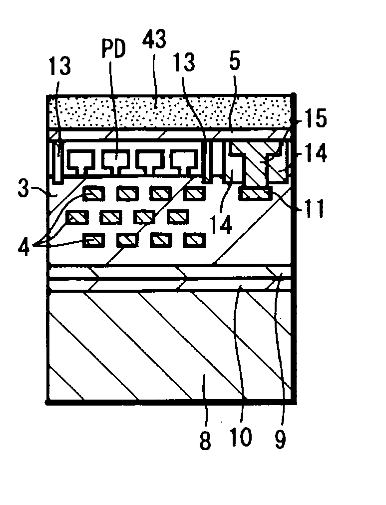
[0109]FIG. 4 is a schematic diagram (cross-sectional view) showing an arrangement of a solid-state imaging device according to an embodiment of the present invention.

[0110] In this embodiment, the present invention is applied to a CMOS type solid-state imaging device having a back-illuminated type structure.

[0111] As shown in FIG. 4, a solid-state imaging device 1 includes a silicon layer 2 in which a photodiode PD serving as a light-receiving sensor portion is formed. A color filter 6 is formed on the silicon layer 2 through a planarized layer 5 and an on-chip lens 7 is formed on the color filter 6. Also, an interconnection portion in which interconnection layers 4 of a plurality of layers (three layers in FIG. 4) are formed within an insulating layer 3 is formed under the silicon layer 2. The interconnection portion is formed on a supporting substrate 8 and the whole of this solid-state ...


PUM


Abstract

A solid state imaging device having a back-illuminated type structure in which a lens is formed on the back side of a silicon layer with a light-receiving sensor portion being formed thereon. Insulating layers are buried into the silicon layer around an image pickup region, with the insulating layer being buried around a contact layer that connects an electrode layer of a pad portion and an interconnection layer of the surface side. A method of manufacturing such a solid-state imaging device is also provided.

Description

BACKGROUND OF THE INVENTION [0001] 1. Field of the Invention [0002] The present invention relates to a solid-state imaging device having a so-called back-illuminated structure for illuminating light on a light-receiving sensor portion from the back side opposite to electrodes and interconnections and a method of manufacturing such a back-illuminated type solid-state imaging device. [0003] 2. Description of the Related Art [0004] It has been customary that a solid-state imaging device has a surface-illuminated type structure with electrodes and interconnections formed on a substrate to illuminate light on a light-receiving sensor portion from above the electrodes and the interconnections. [0005]FIG. 1 of the accompanying drawings is a schematic cross-sectional view showing a solid-state imaging device having a surface-illuminated type structure. [0006] A solid-state imaging device, generally depicted by the reference numeral 50 in FIG. 1, is a CMOS (complementary metal-oxide semicond...

Claims


Application Information

Patent Timeline
Patent Type & Authority Applications(United States)
IPC IPC(8): H01L27/14H01L27/146H01L27/148H01L31/10
CPCH01L27/14601H01L27/14625H01L27/14627H01L27/14632Y10S438/975H01L27/14687H01L27/14689H01L27/1464H01L27/14643H01L21/76898H01L23/481H01L2924/0002H01L2924/00H01L27/14H01L31/10
Inventor YAMAMOTO, YUICHIIWAMOTO, HAYATO
Owner SONY CORP
Why Eureka
Try Eureka