Display device

a display device and display technology, applied in the field of display devices, can solve the problems of reducing yield, reducing line resistance, and reducing the degree of integration of pixels, so as to achieve the effect of increasing line resistance and reliable repair

Inactive Publication Date: 2005-05-26
SANYO ELECTRIC CO LTD
View PDF5 Cites 16 Cited by
  • Summary
  • Abstract
  • Description
  • Claims
  • Application Information

AI Technical Summary

Benefits of technology

[0013] An advantage of the present invention is the disconnection which is a deficient defect can be reliably repaired while the increase in line resistance is inhibited.
[0014] According to one aspect of the present invention, there is provided a display device comprising, a plurality of pixels each having a display element and a plurality of line patterns for supplying power from a same power supply to the plurality of pixels, wherein, in a deficient defect portion of the line pattern, ends of the deficiency are connected to each other with a pattern of a conductive material for repair directly covering the ends, and an insulating film is formed covering the plurality of line patterns and the pattern of conductive material for repair.
[0015] According to another aspect of the present invention, it is preferable that, in the display de

Problems solved by technology

In actual practice, however, because of increases in the resolution and size of display devices, the number of pixels and the degree of integration have increased such that total prevention of the occurrence of defects in the TFT or in the line remains impossible.
If all of substrates (panels) in which a defect occurs in the element formed on one panel or in the line pattern, such as a line, formed on one panel are discarded, the yield would be significantly reduced and the manufacturing cost would be significantly increased.
In the related art, defects in the active matrix liquid crystal display devices are found after almost all of the circuit elements to be formed on one substrate have been formed, by, for example, sequentially selecting each pixel and causing that pixel to display.
However, because

Method used


Image

  • Display device
  • Display device
  • Display device

Examples


Embodiment Construction

[0032] Preferred embodiments of the present invention (hereinafter referred to simply as “embodiments”) will now be described referring to the drawings.

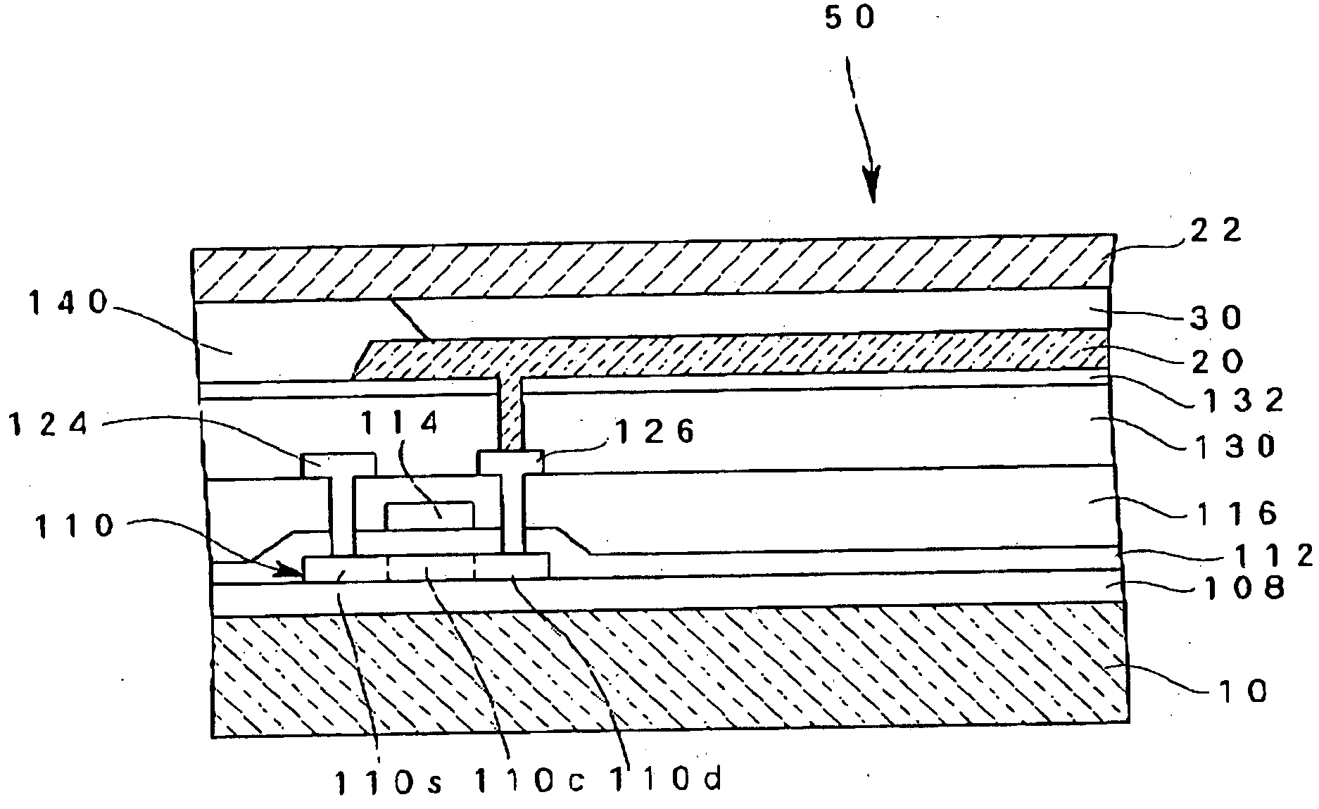
[0033] A display device according to a first preferred embodiment of the present invention is applied to an active matrix display device having a display element and a TFT for driving the display element in each pixel and will be hereinafter described exemplifying an active matrix electroluminescence (hereinafter simply referred to as “EL”) element which uses an EL element as the display element and has an organic EL element and a TFT for controlling and driving the organic EL element in each pixel.

[0034] Among various active matrix display devices, because an active matrix display device which uses an EL element, in particular, an organic EL element having an organic material as a light emitting material is self-emissive and requires no light source, a display device having a thinner thickness than an LCD or the like can be realiz...


PUM


Abstract

Immediately after formation of, for example, power supply lines formed on a same substrate and set to a same potential, defect examination is applied and a repair line is formed connecting deficient defect (disconnection) portion of the power supply line, directly covering the power supply line. The repair line can be formed through a drawing process by scanning with a laser beam within a gas atomospshere of a conductive material such as, for example, tungsten, to connect ends of the disconnection. By repairing the power supply line by directly covering the power supply line, an increase in a line resistance is inhibited and flatness above the repair line is further improved.

Description

CROSS-REFERENCE TO RELATED APPLICATIONS [0001] The priority Japanese Patent Application Number 2003-342049 upon which this patent application is based is hereby incorporated in its entirety by reference.BACKGROUND OF THE INVENTION [0002] 1. Field of the Invention [0003] The present invention relates to the repairing of a defective circuit line pattern in a semiconductor device such as a display device. [0004] 2. Description of the Related Art [0005] As one example of a semiconductor device, an active matrix display device is well-known in which a thin film transistor (hereinafter simply referred to as “TFT”) for driving a display element is provided for each pixel. Among such active matrix display devices, an active matrix liquid crystal display device (hereinafter simply referred to as “LCD”) in which liquid crystal is used as the display element is currently widely in use for various high resolution display devices, including computer monitors and television screens. In such an ac...

Claims


Application Information

Patent Timeline
IPC IPC(8): G02F1/133G02F1/136G02F1/1343G02F1/1362G09F9/00G09G3/04G09G3/32G09G3/36H01L27/32H01L29/786H01L51/50H05B33/14H05B33/26
CPCG02F2001/136263G02F2001/136272G09G3/3208H01L2251/568G09G2330/08H01L27/3258H01L27/3276G09G2300/08G02F1/136272G02F1/136263H10K59/124H10K59/131H10K71/861H05B33/26
Inventor JINNO, YUSHI
Owner SANYO ELECTRIC CO LTD
Why Eureka
Try Eureka