Scanning signal line drive circuit, display device having the same, and driving method for scanning signal line

a drive circuit and signal line technology, applied in the direction of pulse generators, pulse techniques, instruments, etc., can solve the problems of deterioration in the reliability of transistors, video signals indicative of pixel voltage values of a plurality of rows cannot be transmitted by each source line at once, etc., to reduce power consumption, reduce the size of the first-node-turn-off switching element and the output-node-turn-off switching element, the effect of reducing power consumption

Inactive Publication Date: 2014-04-24
SHARP KK
View PDF6 Cites 42 Cited by
  • Summary
  • Abstract
  • Description
  • Claims
  • Application Information

AI Technical Summary

Benefits of technology

[0102]According to the first aspect of the present invention, in a predetermined period of two horizontal scanning periods or longer in each vertical scanning period, the potential of the second node in each bistable circuit becomes the off level. Consequently, the duty ratio of the potential applied to the control terminal of the first-node-turn-off switching element and the control terminal of the output-node-turn-off switching element is substantially reduced more than that in the conventional technique. Consequently, the threshold shift in the first-node-turn-off switching element and the output-node-turn-off switching element is suppressed. By increasing the reliability of the first-node-turn-off switching element and the output-node-turn-off switching element, the size of the first-node-turn-off switching element and the output-node-turn-off switching element can be reduced. By reducing the size of the first-node-turn-off switching element and the output-node-turn-off switching element, power consumption can be reduced. Consequently, while reducing power consumption, the reliability of the first-node-turn-off switching element and the output-node-turn-off switching element can be increased. Further, by reducing the size of the first-node-turn-off switching element and the output-node-turn-off switching element, the size of the scanning signal line drive circuit can be reduced.
[0103]According to the second aspect of the present invention, in the predetermined period, supply of a clock signal to a bistable circuit is stopped. Therefore, in the predetermined period, the potential of the first node and the potential of the second node are reliably maintained at the low level. Accordingly, the potential of the second node in each bistable circuit is reliably maintained at the off level. Therefore, the duty ratio of the potential of the second node in each bistable circuit is reliably decreased from that in the conventional technique. As a result, by reliably suppressing the threshold shift in the first-node-turn-off switching element and the output-node-turn-off switching element, the reliability of the elements can be reliably increased.
[0104]According to the third aspect of the present invention, the longer the predetermined period is, the higher the frequency of the clock signal is. Consequently, the length of one vertical scanning period is constant. Therefore, without decreasing a substantive drive frequency, the reliability of the first-node-turn-off switching element and the output-node-turn-off switching element can be increased.
[0105]According to the fourth aspect of the present invention, after power-on, the potential of the first node and the potential of the second node are reset to the off level. Further, in a period after power-on until the start time point of a first vertical scanning period, supply of a clock signal to a bistable circuit is stopped. Consequently, the potential of the first node and the potential of the second node are reliably maintained at the off level. Therefore, the circuit operation can be made more stable.
[0106]According to the fifth aspect of the present invention, the clock control circuit controls supply of a clock signal to a bistable circuit based on the end signal. Consequently, supply of the clock signal is controlled reliably. Thus, the circuit operation can be stabilized.
[0107]According to the sixth aspect of the present invention, based on the end signal, at the start time of the vertical blanking period, the potential of the second node in each bistable circuit is reliably set to the off level, and the potential of the first node in the bistable circuit in at least the final stage is reliably set to the off level. Consequently, the duty ratio of the potential supplied to the control terminal of the first-node-turn-off switching element and the control terminal of the output-node-turn-off switching element is reliably made lower than that in the conventional technique, and the circuit operation can be further stabilized.

Problems solved by technology

However, video signals indicative of pixel voltage values of a plurality of rows cannot be transmitted by each source line at once (simultaneously).
As a result, the threshold shift which occurs in the transistors M5 and M6 becomes large, and it causes deterioration in the reliability of the transistors.

Method used


Image

  • Scanning signal line drive circuit, display device having the same, and driving method for scanning signal line
  • Scanning signal line drive circuit, display device having the same, and driving method for scanning signal line
  • Scanning signal line drive circuit, display device having the same, and driving method for scanning signal line

Examples


first embodiment

1. First Embodiment

1.1 General Configuration and Operation

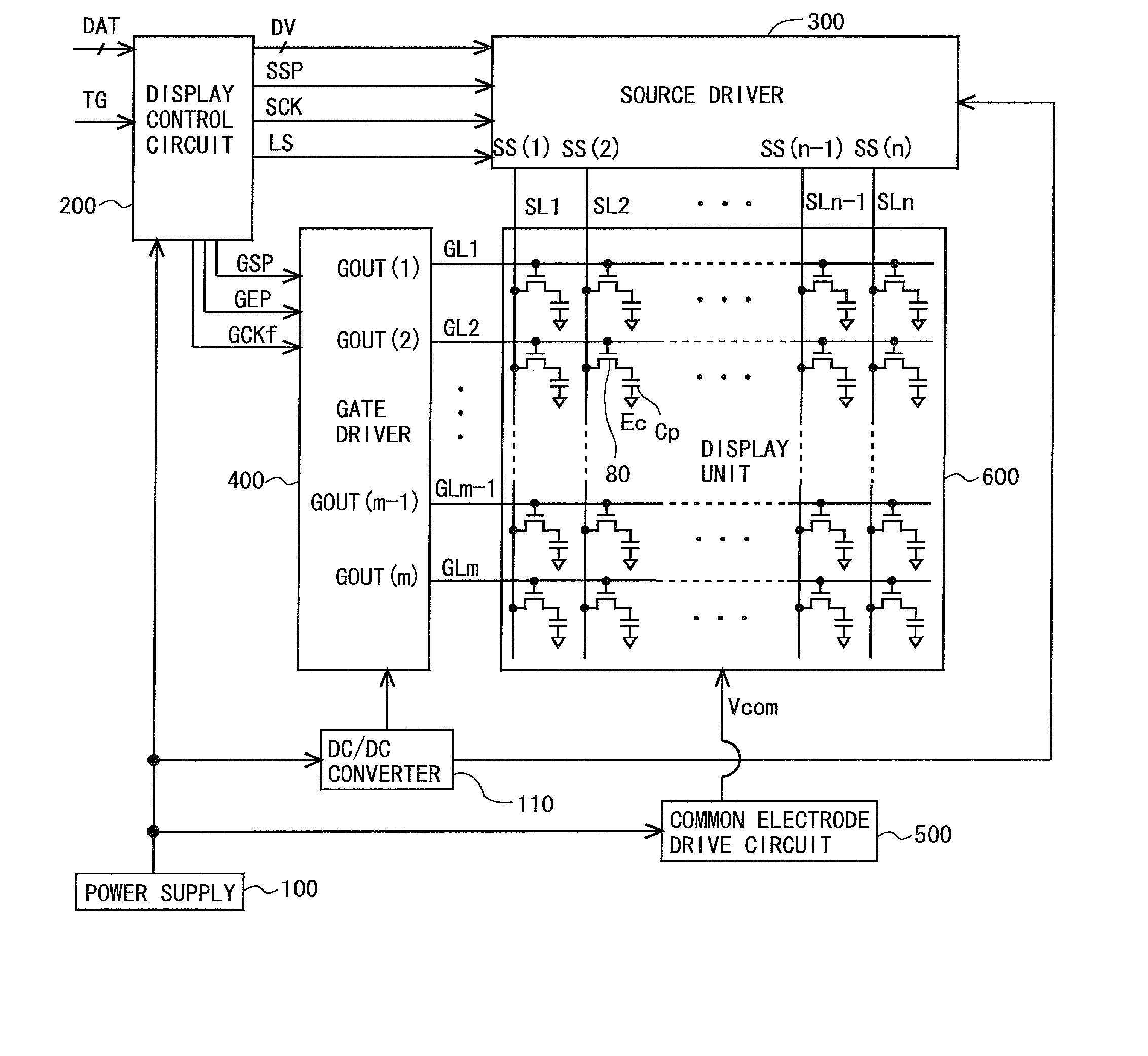
[0155]FIG. 1 is a block diagram illustrating a general configuration of an active matrix-type liquid crystal display device according to a first embodiment of the present invention. As illustrated in FIG. 1, the liquid crystal display device includes a power supply 100, a DC / DC converter 110, a display control circuit 200, a source driver (video signal line drive circuit) 300, a gate driver (scanning signal line drive circuit) 400, a common electrode drive circuit 500, and a display unit 600. It should be noted that the gate driver 400 is formed on a display panel including the display unit 600 by using amorphous silicon, polycrystal silicon, microcrystal silicon, oxide semiconductor (for example, IGZO), or the like. That is, in the present embodiment, the gate driver 400 and the display unit 600 are formed on the same substrate (array substrate as one of two substrates constituting the liquid crystal panel). Consequently, th...

second embodiment

2. Second Embodiment

2.1 Detailed Operation of Gate Driver

[0214]FIG. 22 is a signal waveform diagram for explaining the detailed operation of the gate driver 400 in a second embodiment of the present invention. It should be noted that, since the general configuration and operation of a liquid crystal display device, the configuration of the gate driver 400, the configuration and operation of a bistable circuit, and the configuration and operation of the clock control circuit 420 in the present embodiment are similar to those of the first embodiment, their description will not be given.

[0215]In the first embodiment, the vertical blanking period (about 8.3 msec) whose length is about 1 / 2 of one vertical scanning period is provided, and the drive frequency in the write period is set to 120 Hz (about 8.3 msec) which is twice as high as the general drive frequency (60 Hz). On the other hand, in the present embodiment, as illustrated in FIG. 22, a vertical blanking period (about 11.1 msec)...

third embodiment

3. Third Embodiment

3.1 Detailed Operation of Gate Driver

[0217]FIG. 23 is a signal waveform diagram for explaining the detailed operation of the gate driver 400 in a third embodiment of the present invention. It should be noted that, since the general configuration and operation of a liquid crystal display device, the configuration of the gate driver 400, the configuration and operation of a bistable circuit, and the configuration and operation of the clock control circuit 420 in the present embodiment are similar to those of the first embodiment, their description will not be given.

[0218]In the first embodiment, the vertical blanking period (about 8.3 msec) whose length is about 1 / 2 of one vertical scanning period is provided, and the drive frequency in the write period is set to 120 Hz (about 8.3 msec) which is twice as high as the general drive frequency (60 Hz). In the second embodiment, the vertical blanking period (about 11.1 msec) whose length is about 2 / 3 of one vertical scan...


PUM


Abstract

The purpose of this invention is to increase reliability of a switching element while reducing consumption power. In the vertical blanking period, an end pulse signal (ED) changes from the low level to the high level. The potential of first nodes (N1) in the first stage to (m−1)th stage of cascade-connected m-stage bistable circuits included in a shift register of the scanning signal drive circuit is reliably maintained at the low level, and the potential of second nodes (N2) in the first stage to the (m−1)th stage changes from the high level to the low level. In a bistable circuit in the m-th stage, the potential of the first node (N1) in the m-th stage changes from the high level to the low level, and the potential of the second node (N2) in the m-th stage is maintained at the low level. The supply to a bistable circuit of clock signals (CKA, CKB) is stopped. Until a write period in the subsequent vertical scanning period, the potential of the first node (N1) and the potential of the second node (N2) in each stage are maintained at the low level.

Description

TECHNICAL FIELD[0001]The present invention relates to a scanning signal line drive circuit, a display device having the same, and a driving method for a scanning signal line and, particularly, to a scanning signal line drive circuit suitable for monolithic fabrication, a display device having the same, and a driving method for a scanning signal line by the scanning signal line drive circuit.BACKGROUND ART[0002]Conventionally, a gate driver (a scanning signal line drive circuit) for driving gate lines (scanning signal lines) of a liquid crystal display device is often mounted as an IC (Integrated Circuit) chip in a peripheral portion of a substrate constituting a liquid crystal panel. In recent years, however, formation of a gate driver directly on a substrate is gradually increasing. Such a gate driver is called a “monolithic gate driver” or the like.[0003]In a liquid crystal display device having a monolithic gate driver, a thin film transistor using amorphous silicon (a-Si) (herei...

Claims


Application Information

Patent Timeline
Patent Type & Authority Applications(United States)
IPC IPC(8): H03K3/012G09G3/36
CPCG09G3/3696H03K3/012G09G3/3677G09G2310/0286G11C19/28G02F1/133G09G3/20G09G3/36
Inventor IWASE, YASUAKI
Owner SHARP KK
Why Eureka
Try Eureka