
Circuit module

a circuit module and circuit technology, applied in the field of circuit modules, can solve the problems of small solder balls, difficult to electrically connect these elements using a leadframe, and active elements such as lsi and/or trs,

Inactive Publication Date: 2005-06-02
SANYO ELECTRIC CO LTD +1
View PDF10 Cites 32 Cited by
  • Summary
  • Abstract
  • Description
  • Claims
  • Application Information

AI Technical Summary

Benefits of technology

The present invention provides a circuit module with leads and a fine pattern. The module has a mount board that absorbs mechanical stress and incorporates a high-performance system. The circuit device has a conductive pattern with an interval smaller than that between the leads. The module also includes a first circuit element sealed with first sealing resin, a second circuit element fixed to an island attached to one of the leads, and second sealing resin for sealing the mount board and the first and second circuit elements. The mount board has a conductive pattern with an interval smaller than that between the leads. The second sealing resin has a larger thermal expansion coefficient than the first sealing resin.

Problems solved by technology

However, a leadframe-type package has the problem that active elements, such as an LSI and / or TRs, and passive elements, such as chip capacitors, cannot be simultaneously incorporated therein.
This is because it is difficult to electrically connect these elements using a leadframe.
However, since the SIP-type package is thin and small, solder balls are small.
This causes the problem that, when the SIP is mounted on a printed-circuit board or the like, cracks occur in the solder balls due to the difference in thermal expansion coefficients between the mount board and the package.
Further, when the SIP is realized as a high-performance semiconductor element in an atmosphere in which heat is produced, e.g., an on-vehicle environment or the like, problems occur in terms of heat dissipation and electrical connection.
This causes the problem that a complex electrical circuit cannot be constructed inside the circuit device using the leads 101.

Method used


Image

  • Circuit module
  • Circuit module
  • Circuit module

Examples


Embodiment Construction

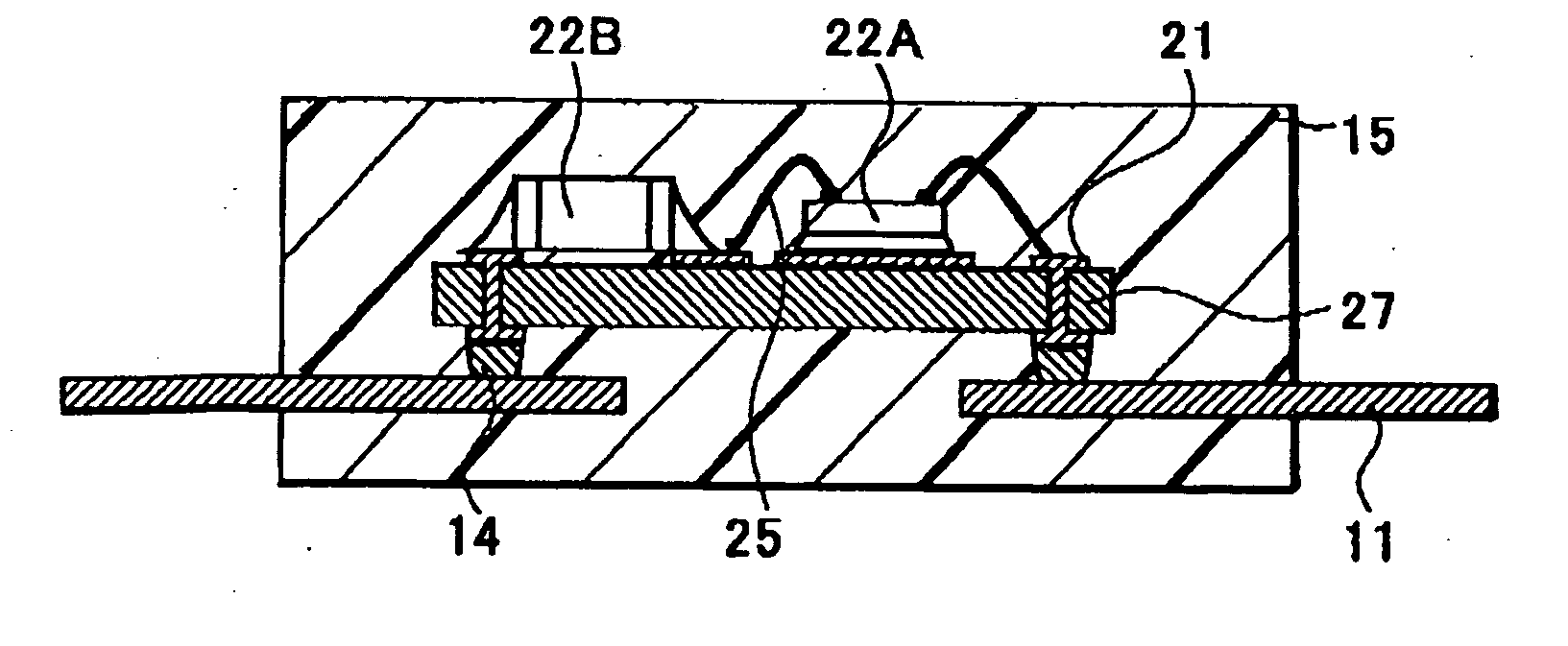
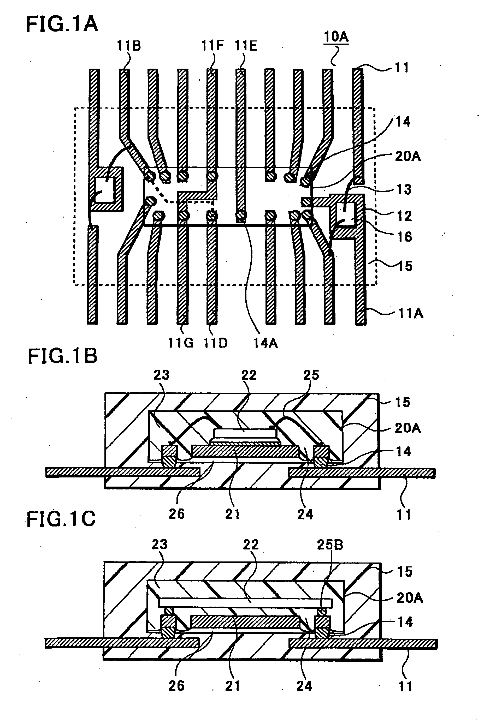
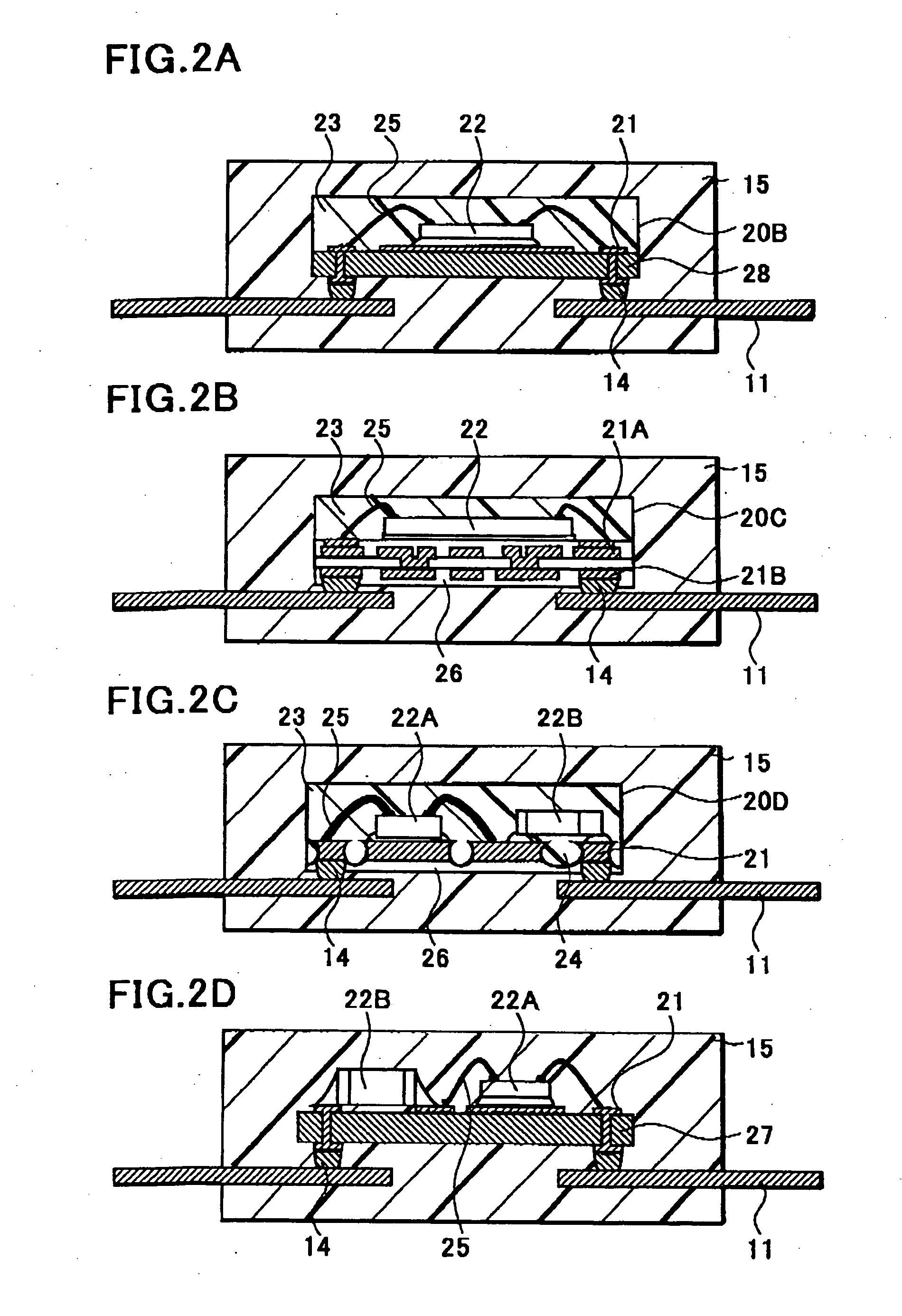
[0025] The structure of a circuit module 10A of the preferred embodiments of the present invention will be described with reference to FIG. 1A and FIG. 1B. FIG. 1A is a plan view of the circuit module 10A, and FIG. 1B is a cross-sectional view thereof.

[0026] As can be seen from these drawings, the circuit module 10A of a preferred embodiment has a structure in which a thin-type circuit device, such as a SIP, provided with external connection electrodes is mounted on a leadframe and sealed with resin. This structure allows a large number of elements to be simultaneously incorporated therein and makes it possible to realize a module in which leads are adopted with a circuit device in which external electrodes can only be provided on the back surface thereof. Even when the circuit module 10A is mounted on a printed-circuit board, a ceramic board, or a metal board (hereinafter referred to as a mount board), thermal stress is reduced by the leads 11, and furthermore, heat release proper...


PUM


Abstract

A circuit module of the present invention has leads serving as terminals for performing electrical input from, and output to exterior, a circuit device in which a first circuit element electrically connected to at least one of the leads is sealed with first sealing resin, a second circuit element fixed to an island formed in one of the leads, and second sealing resin for sealing the circuit device and the second circuit element. Here, the circuit device has a conductive pattern with an interval smaller than that between the leads.

Description

BACKGROUND OF THE INVENTION [0001] Priority is claimed to Japanese Patent Application Serial No. JP2003-204297, filed on Jul. 31, 2003, and JP2004-205793, filed on Jul. 13, 2004, the disclosures of which are incorporated herein by reference in its entireties. [0002] 1. Field of the Invention [0003] The present invention relates to a circuit module. In particular, the present invention relates to a circuit module having leads as external terminals. [0004] 2. Description of the Related Arts [0005] With reference to FIG. 9A and FIG. 9B, the structure of a conventional-type circuit device 100 will be described. FIG. 9A is a plan view of the circuit device 100, and FIG. 9B is a cross-sectional view thereof. [0006] A land 102 made of conductive material is formed in the center of the circuit device 100, and one ends of a large number of leads 101 are close to the periphery of the land 102. The one ends of the leads 101 are electrically connected to a semiconductor element 104 through fine...

Claims


Application Information

Patent Timeline
Patent Type & Authority Applications(United States)
IPC IPC(8): H01L23/29H01L23/12H01L23/31H01L23/495H01L23/50H01L25/04H01L25/18
CPCH01L23/3135H01L2924/12041H01L23/49537H01L23/49562H01L23/49575H01L2224/48091H01L2224/48247H01L2224/73265H01L2924/01078H01L2924/01079H01L2924/13055H01L2924/13091H01L2924/15311H01L2924/19041H01L2924/19105H01L2924/19107H01L23/49531H01L2224/16245H01L2224/48227H01L2924/07802H01L2224/32245H01L2224/32225H01L24/48H01L2924/00014H01L2924/00H01L2924/00012H01L2224/451H01L24/45H01L24/73H01L2924/181H01L2224/45099H01L2224/05599H01L23/50H01L23/495
Inventor SANDO, FUMIOIGARASHI, YUSUKESAKAMOTO, NORIAKI
Owner SANYO ELECTRIC CO LTD
Learn More