MIM capacitor having flat diffusion prevention films

a technology of diffusion prevention and capacitor, which is applied in the direction of capacitors, solid-state devices, transistors, etc., can solve the problems of structure and process of mim capacitor, and achieve the effects of preventing leakage current, reducing electrode area, and large diffusion coefficien

Inactive Publication Date: 2005-05-17
KK TOSHIBA
View PDF11 Cites 27 Cited by
  • Summary
  • Abstract
  • Description
  • Claims
  • Application Information

AI Technical Summary

Benefits of technology

[0008]It is an object of the present invention to provide a manufacturing process for satisfactorily preventing the leakage current even when the electrode of a MIM capacitor is formed from a material such as Cu having a large diffusion coefficient, and avoiding dishing and reduction in electrode area even when the damascene process (CMP process) is employed.

Problems solved by technology

The first problem in integrating the processes is the structure and process of a MIM capacitor.
At this time, the electrode of the MIM capacitor is also formed by the damascene process, and thus suffers problems caused by the damascene process, e.g., dishing and reduction in electrode area in avoiding dishing.

Method used


Image

  • MIM capacitor having flat diffusion prevention films
  • MIM capacitor having flat diffusion prevention films
  • MIM capacitor having flat diffusion prevention films

Examples


first embodiment

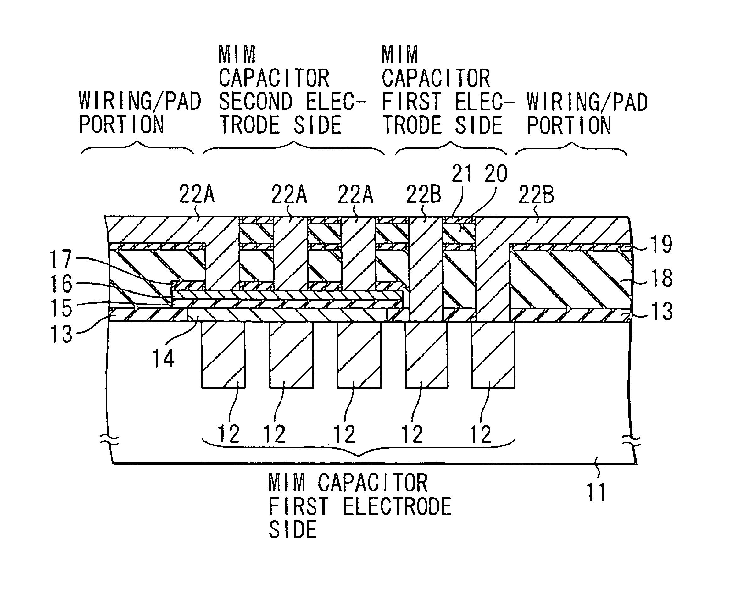
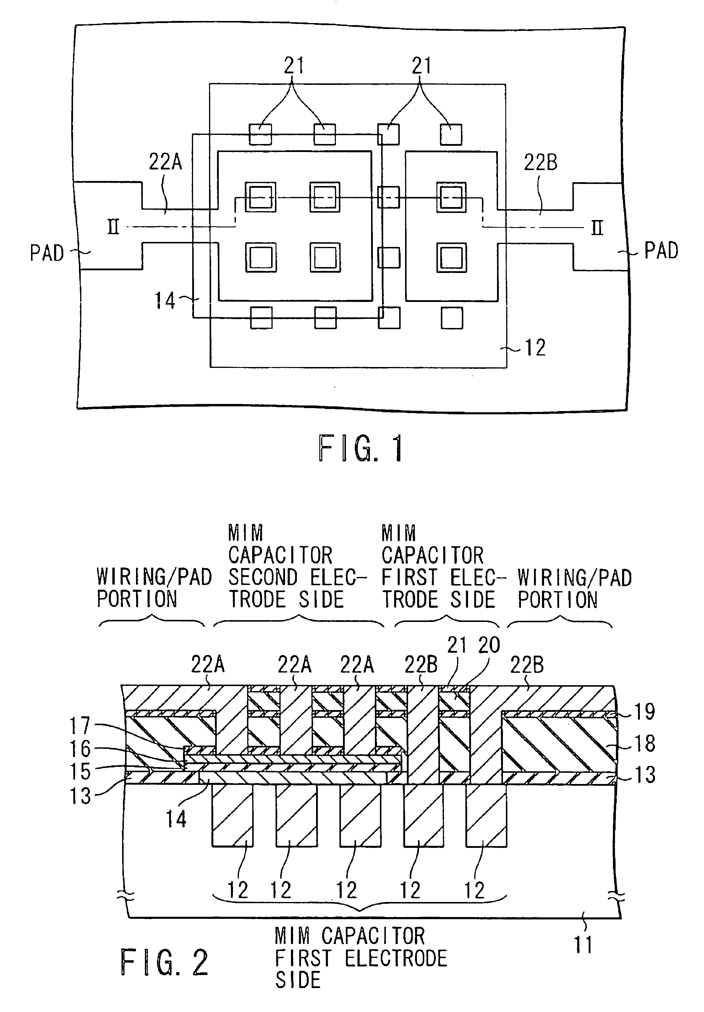
[0059]FIG. 1 is a sectional view showing a MIM capacitor according to the present invention. FIG. 2 is a sectional view taken along the line II—II in FIG. 1.

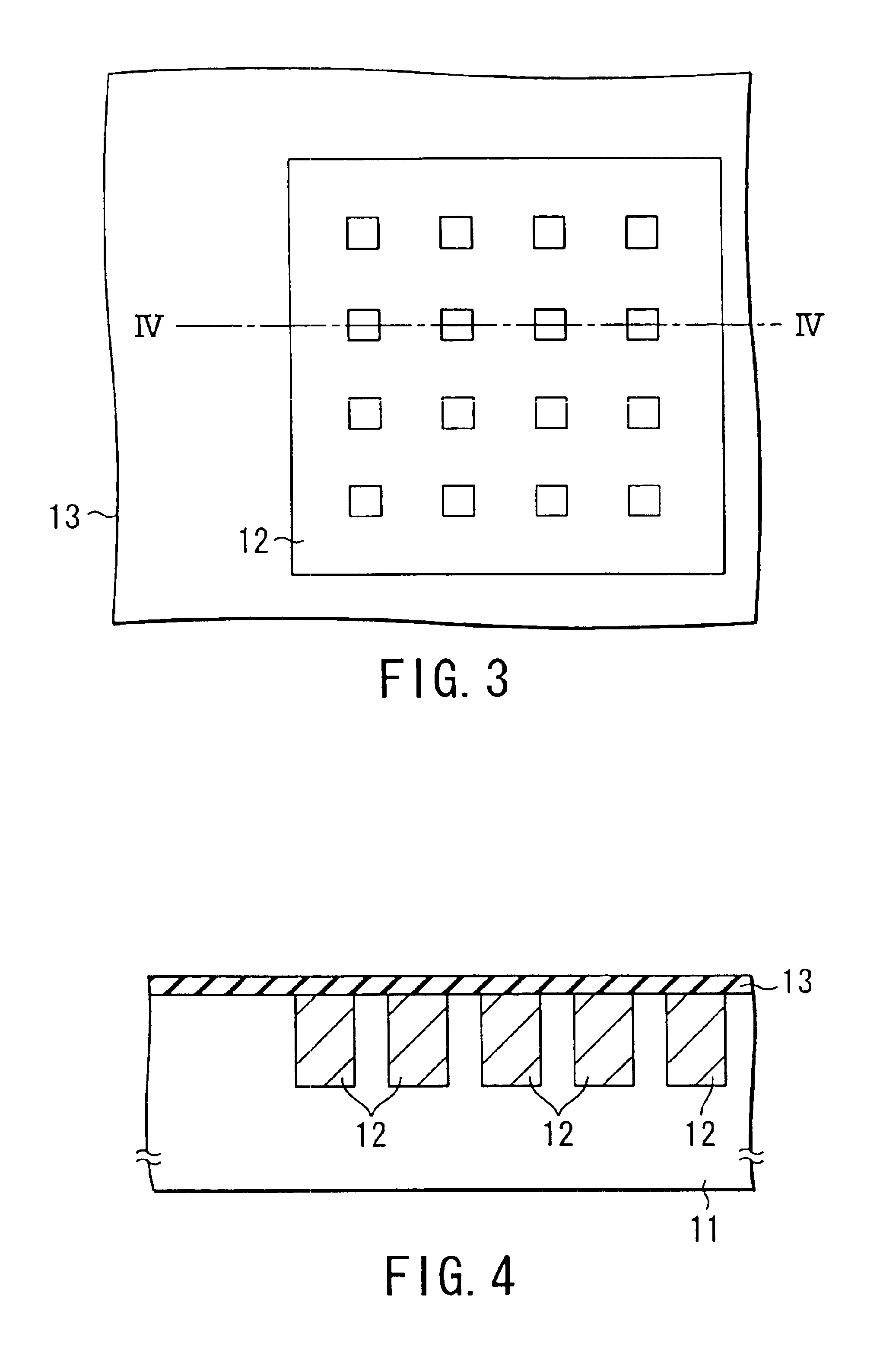
[0060]For example, a matrix-like trench is formed in a semiconductor substrate (e.g., silicon substrate) 11. The trench is filled with a metal material 12, e.g., Cu (copper) having a low resistance and large diffusion coefficient. The metal material 12 filled in the trench of the semiconductor substrate 11 serves as the first electrode of the MIM capacitor.

[0061]The first embodiment adopts a matrix shape as the layout of the first electrode of the MIM capacitor in order to prevent dishing (phenomenon that a metal material in a trench is polished like a dish) in the damascene process (CMP process). As far as the structure can prevent dishing, the trench shape is not limited to the matrix shape, and may be a drainboard (or ladder) or comb shape.

[0062]A silicon nitride film (SiN) 13 is formed on the semiconductor substrate 11 excep...

second embodiment

[0093]FIG. 16 shows a MIM capacitor according to the present invention.

[0094]Compared to the embodiment in FIGS. 1 and 2, the device structure of the second embodiment is characterized by the absence of the silicon nitride film 13 in FIGS. 1 and 2. In other words, in the second embodiment, a silicon nitride film 17 is formed not only on a tungsten nitride film 16 but also on a semiconductor substrate 11 and metal material 12.

[0095]The detailed structure will be explained.

[0096]For example, a matrix-like trench is formed in a semiconductor substrate (e.g., silicon substrate) 11. The trench is filled with a metal material 12, e.g., Cu (copper) having a low resistance and large diffusion coefficient. The metal material 12 filled in the trench of the semiconductor substrate 11 serves as the first electrode of the MIM capacitor.

[0097]Note that the shape of the first electrode of the MIM capacitor is set to a matrix shape, drainboard shape (or ladder shape), comb shape, or the like.

[0098]...

third embodiment

[0127]FIG. 21 shows a MIM capacitor according to the present invention.

[0128]Compared to the embodiment in FIGS. 1 and 2, the device structure of the third embodiment is characterized by the layout of a tungsten nitride film 14 serving as a diffusion prevention film. More specifically, in this embodiment, the tungsten nitride film 14 as a diffusion prevention film is etched subsequently to etching of a silicon nitride film 17, tungsten nitride film 16, and capacitor insulating film 15. The device structure of this embodiment has a layout in which the ends of the tungsten nitride films 14 and 16, and capacitor insulating film 15 overlap a silicon nitride film 13.

[0129]Accordingly, the third embodiment can eliminate the step (CMP) of filling the tungsten nitride film 14 in the groove of the silicon nitride film 13 shown in the embodiment of FIGS. 1 and 2.

[0130]The detailed device structure will be explained.

[0131]For example, a matrix-like trench is formed in a semiconductor substrate...


PUM


Abstract

At present, Cu (copper) is being used as a wiring material. In an RF-CMOS device as a combination of an RF analog device and CMOS logic device, two electrodes of a MIM capacitor are formed from Cu having a large diffusion coefficient. To prevent Cu from diffusing to the capacitor insulating film of the MIM capacitor, diffusion prevention films having a function of preventing diffusion of Cu are interposed between the capacitor insulating film and the two electrodes. As a result, Cu forming the electrodes does not diffuse to the capacitor insulating film.

Description

CROSS-REFERENCE TO RELATED APPLICATIONS[0001]This application is based upon and claims the benefit of priority from the prior Japanese Patent Applications No. 11-354473, filed Dec. 14, 1999; No. 2000-368693, filed Dec. 4, 2000, the entire contents of which are incorporated herein by reference.BACKGROUND OF THE INVENTION[0002]The present invention relates to a MIM (Metal-Insulator-Metal) capacitor.[0003]In recent years, for example, the plausibility of forming an RF analog device and CMOS logic device on one chip is being examined. The RF analog device includes a resistor, coil, and capacitor, whereas the CMOS logic device is formed from a MOS transistor.[0004]To form an RF analog device and CMOS logic device on one chip, the manufacturing processes of these devices must be integrated. For example, the process of the RF analog device is integrated based on the CMOS logic process to develop a new RF-CMOS process.[0005]The first problem in integrating the processes is the structure and...

Claims


Application Information

Patent Timeline
Patent Type & Authority Patents(United States)
IPC IPC(8): H01L21/02H01L27/08H01L27/06H01L27/04H01L21/822
CPCH01L27/0629H01L28/60H01L27/0805H01L27/04
Inventor YOSHITOMI, TAKASHIOHGURO, TATSUYAHASUMI, RYOJIKIMIJIMA, HIDEKIYAMAGUCHI, TAKASHIINOHARA, MASAHIRO
Owner KK TOSHIBA
Why Eureka
Try Eureka