Method using conductive atomic force microscopy to measure contact leakage current

a technology of atomic force microscopy and contact leakage current, which is applied in the direction of individual semiconductor device testing, semiconductor/solid-state device testing/measurement, instruments, etc., can solve the problems of large leakage current, large leakage current, and defective contacts that are produced

Inactive Publication Date: 2005-06-16
TAIWAN SEMICON MFG CO LTD
View PDF21 Cites 15 Cited by
  • Summary
  • Abstract
  • Description
  • Claims
  • Application Information

AI Technical Summary

Problems solved by technology

Sometimes, during the contact fabrication process, defective contacts are produced.
The defective contacts are often characterized by larger leak currents.
The larger leak currents may also be due to defects in the structures of the semiconductor device, such as the gate oxide.
Unfortunately, conventional defect detecting techniqu...

Method used


Image

  • Method using conductive atomic force microscopy to measure contact leakage current
  • Method using conductive atomic force microscopy to measure contact leakage current
  • Method using conductive atomic force microscopy to measure contact leakage current

Examples


Embodiment Construction

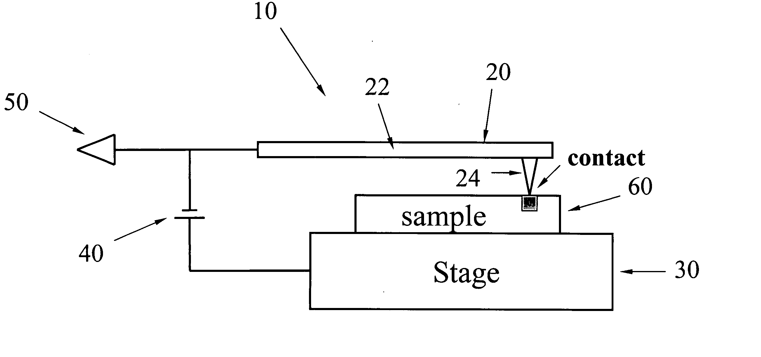
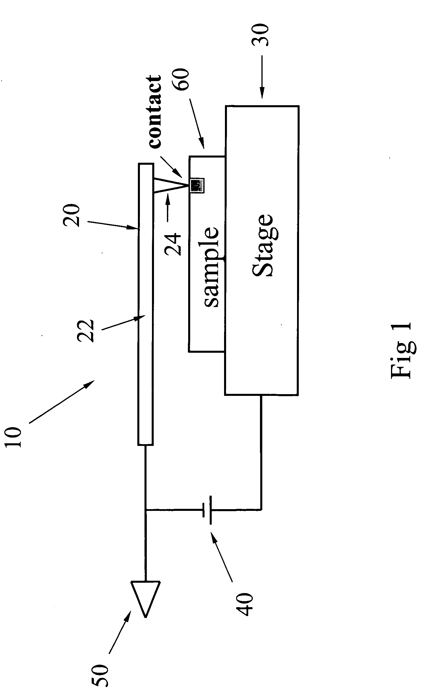
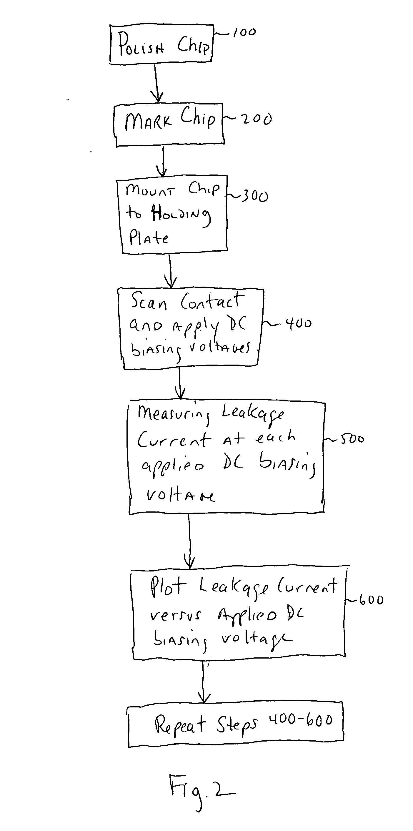
[0012] The present invention is a method for measuring the current leakage (tunneling current) of a contact of a semiconductor device at the nano-ampere level and lower current levels, such as pico-ampere level. This is accomplished in the present invention with conductive atomic force microscopy. The ability to measure the micro-current leakage of a contact allows for high resolution and high sensitivity current mapping of the contact, i.e., current leakage versus applied voltage curve (I / V curve). The resolution and sensitivity of this current mapping is much better than in conventional methods, such as voltage contrast performed on a SEM. Furthermore, the method of the present invention provides a better understanding about the relationship between an abnormal contact and its adjacent contacts through their I / V curves. In addition, the detailed data obtain with the method of the invention allows for the implementation of an appropriate physical failure analysis technology to iden...


PUM


Abstract

A method for measuring current leakage of a contact of a semiconductor device formed on or in a substrate, includes scanning the contact with a probe of a conductive atomic force microscope; applying a DC voltage between the substrate and a conductive tip of the probe; and measuring a value of a current passing through the contact to the substrate, in response to the applied DC voltage.

Description

FIELD OF INVENTION [0001] The present invention relates to integrated circuit defect detection and failure analysis. More specifically, the present invention relates to a method that utilizes conductive atomic force microscopy to measure the contact leak current of a semiconductor device. BACKGROUND OF THE INVENTION [0002] Semiconductor devices have source / drain regions and gate electrodes connected to metal wirings by contact structures. A typical contact structure may be fabricated by forming an interlayer insulating film composed for example, of SiO2, over the semiconductor device and selectively removing a portion of the insulating film to form a contact hole. A metal composite film composed, for example, of titanium (Ti), titanium nitride (TiN) and aluminum (Al) are successively deposited on the surface of the contact hole. After that, the contact hole is filled with a metal, such as tungsten to complete the contact. [0003] During contact fabrication, the Ti film reacts with si...

Claims


Application Information

Patent Timeline
IPC IPC(8): G01Q30/20G01Q60/00G01R31/02G01R31/26G01R31/265H01L21/66
CPCG01R31/2648Y10S977/854G01R31/265G01Q60/40
Inventor LEE, JON C.CHUANG, JUNG-HSIANG
Owner TAIWAN SEMICON MFG CO LTD
Why Eureka
Try Eureka