
Reducing power consumption during MRAM writes using multiple current levels

Inactive Publication Date: 2005-06-16
EVERSPIN TECHNOLOGIES
View PDF8 Cites 13 Cited by
  • Summary
  • Abstract
  • Description
  • Claims
  • Application Information

AI Technical Summary

Problems solved by technology

Disadvantages of Flash memory include high voltage requirements and slow program and erase times. Also, Flash memory has a poor write endurance before memory failure.
Hence, Flash memory is limited in the dimensions to which it can be scaled.
However, in this case there is no “half-select” upon the application of a single field.
Due to the aforementioned constraints, or “windows”, in reliably switching both conventional-mode and toggle-mode MRAM, it is disadvantageous to apply more current during a write than is absolutely necessary to switch the bits.

Method used


Image

  • Reducing power consumption during MRAM writes using multiple current levels
  • Reducing power consumption during MRAM writes using multiple current levels
  • Reducing power consumption during MRAM writes using multiple current levels

Examples


Embodiment Construction

)

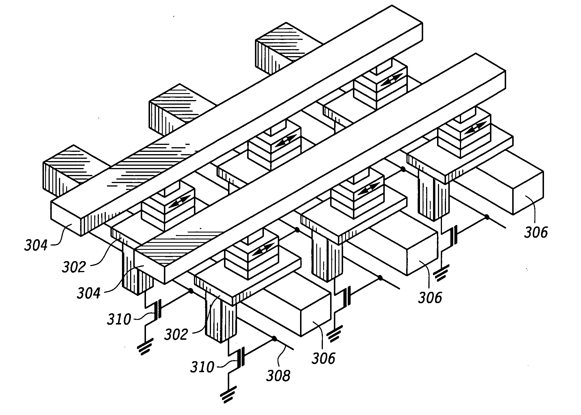
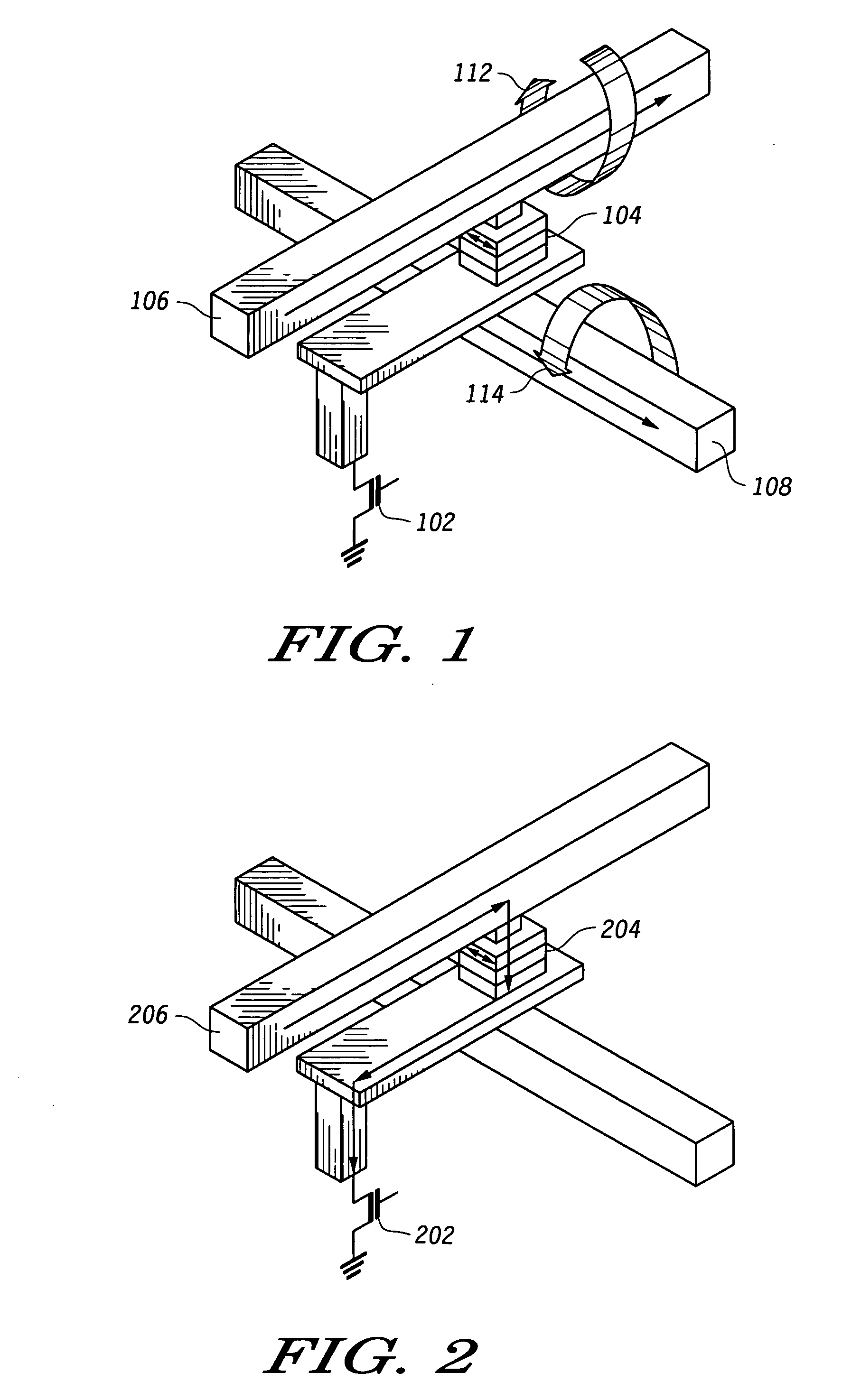
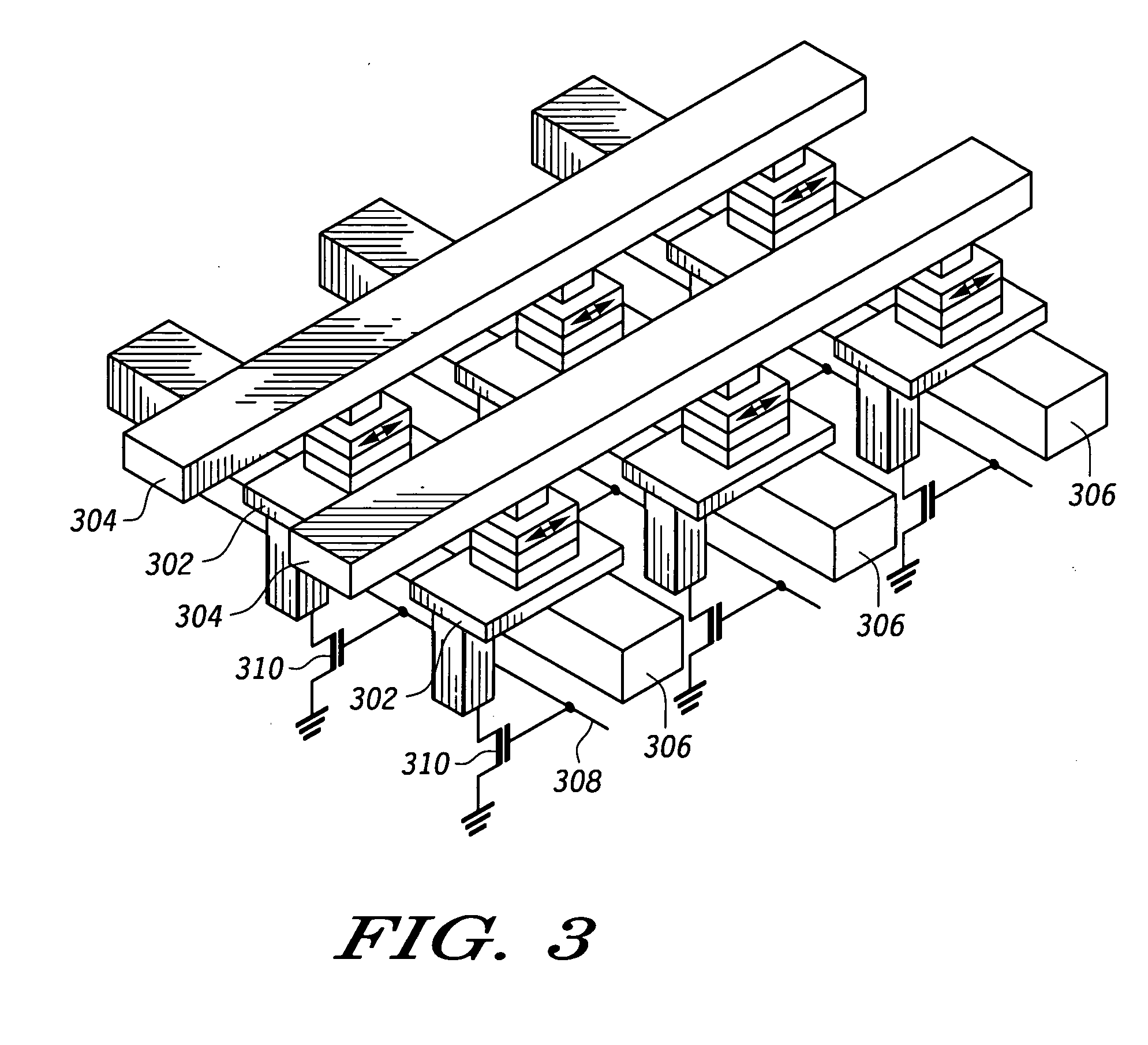
[0022] According to the present disclosure, a reduced power method of writing MRAM bits is disclosed. The reduced power method includes first attempting to write to the MRAM bits using a low magnitude magnetic field and determining if the bit has switched. If the write was not successful, a second, higher magnitude magnetic field is used to write the bit. Applying a magnetic field to an MRAM bits is accomplished by sending a current pulse through a strip line adjacent to the MRAM bits. Thus, lower current pulses can be used for a portion of MRAM bits in an array, saving power consumed.

[0023] Various embodiments are disclosed. In a first embodiment, the above method is performed for every write to an MRAM bit. In another embodiment, the weaker magnetic field is applied during system test or system initialization, and if the weaker field fails to meet an objective, such as to toggle the stored value, an indication of the failed objective is stored and each subsequent write to the MR...


PUM


Abstract

A reduced power method of writing MRAM bits is disclosed. The reduced power method includes writing MRAM bits by applying a first magnetic field having a low magnitude, then determining if the bit has switched. If not, a second magnetic field having a higher magnitude is applied. Applying magnetic fields to an MRAM bit cell is accomplished by sending a current pulse through a strip line adjacent to the MRAM bit cell. The technique can be performed for every write to an MRAM bit. Alternatively, the weaker magnetic field can be applied during system test or system initialization, and if the weaker field fails to write the bit to a desired value, the failing result is stored and each subsequent write to the MRAM bit utilizes the stronger magnetic field.

Description

BACKGROUND [0001] 1. Field of the Disclosure [0002] This disclosure relates to semiconductor memory devices, and, more particularly, to semiconductor random access memory devices that utilize a magnetic field. [0003] 2. Description of the Related Art [0004] Non-volatile memory devices are an important component in electronic systems. Flash memory is the major non-volatile memory device in use today. Typical non-volatile memory devices use charges trapped in a floating oxide layer to store information. Disadvantages of Flash memory include high voltage requirements and slow program and erase times. Also, Flash memory has a poor write endurance before memory failure. In addition, to maintain reasonable data retention, the scaling of the gate oxide is restricted by the tunneling barrier seen by the electrons. Hence, Flash memory is limited in the dimensions to which it can be scaled. [0005] To overcome these shortcomings, magnetic memory devices are being evaluated. One such device is ...

Claims


Application Information

Patent Timeline
IPC IPC(8): G11C11/00G11C11/16
CPCG11C11/16
Inventor DEHERRERA, MARK F.AKERMAN, BENGT JOHAN
Owner EVERSPIN TECHNOLOGIES
Learn More