
Assembled structure of a connector

Inactive Publication Date: 2005-06-16
PLASTRON PRECISION
View PDF6 Cites 5 Cited by
  • Summary
  • Abstract
  • Description
  • Claims
  • Application Information

AI Technical Summary

Benefits of technology

[0003] However, in such an assembled structure of said traditional connector, spring jackwires in the I / O port and beam contacts in the connector socket are connected to terminals on the PCB in a way of welding or pressing, the method is difficult and cost lots of time. Furthermore, in the PCB of such a connector, terminals crossing the PCB will form a through hole structure; which will cause capacitance efficiency and crosstalk among wires. Therefore, an object of the present invention is to solve disadvantages of structure of traditional connector.
[0006] An assembled structure of a connector according to the present invention has the following advantages:
[0009] 3. With the assembled structure of a connector according to the present invention, the spring plate structure formed by spring jackwires in the I / O port and beam contacts in the connector socket enables to said spring plates to change their size or position to match the layout of wires on said PCB; thus crosstalk can be reduced according to the match with layout of wires.
[0010] 4. With the assembled structure of a connector according to the present invention, the spring plate structure formed by spring jackwires in the I / O port and beam contacts in the connector socket can match the layout of wires on the PCB, so the through conductive hole structure through PCB is unnecessary, therefore capacitance efficiency and crosstalk can be avoided.

Problems solved by technology

However, in such an assembled structure of said traditional connector, spring jackwires in the I / O port and beam contacts in the connector socket are connected to terminals on the PCB in a way of welding or pressing, the method is difficult and cost lots of time.

Method used


Image

  • Assembled structure of a connector
  • Assembled structure of a connector
  • Assembled structure of a connector

Examples


Embodiment Construction

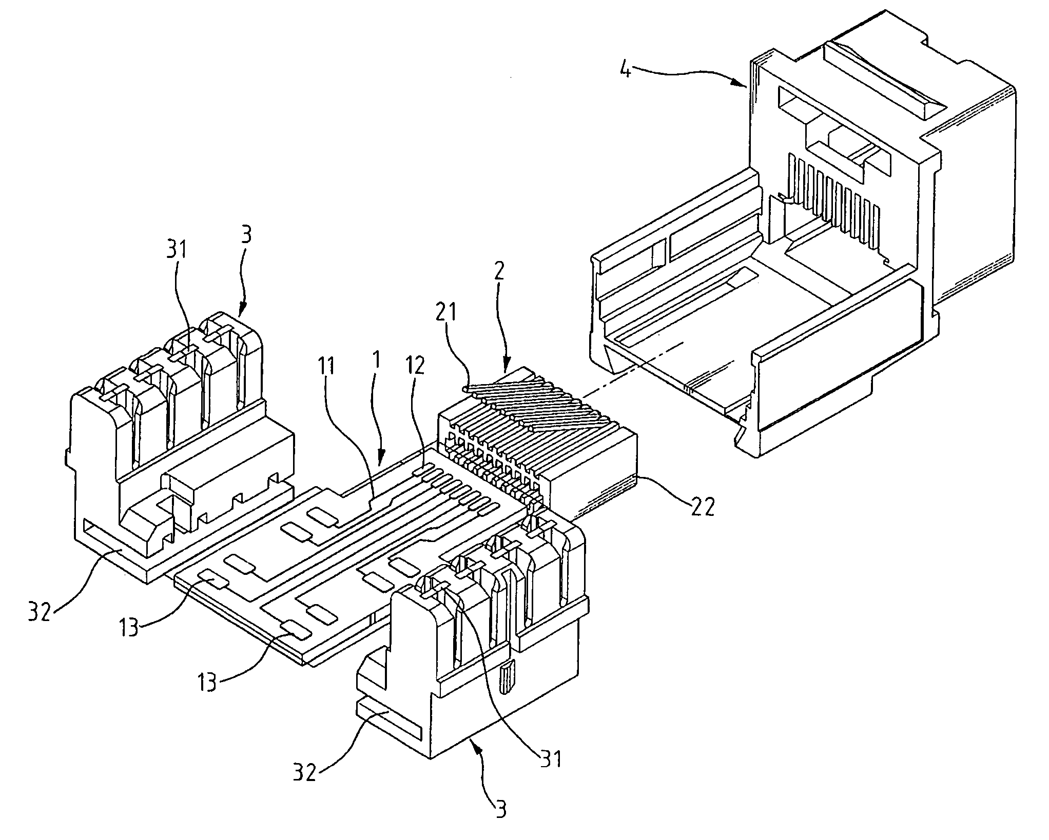
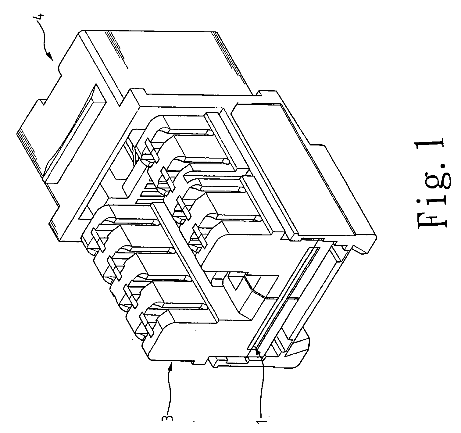
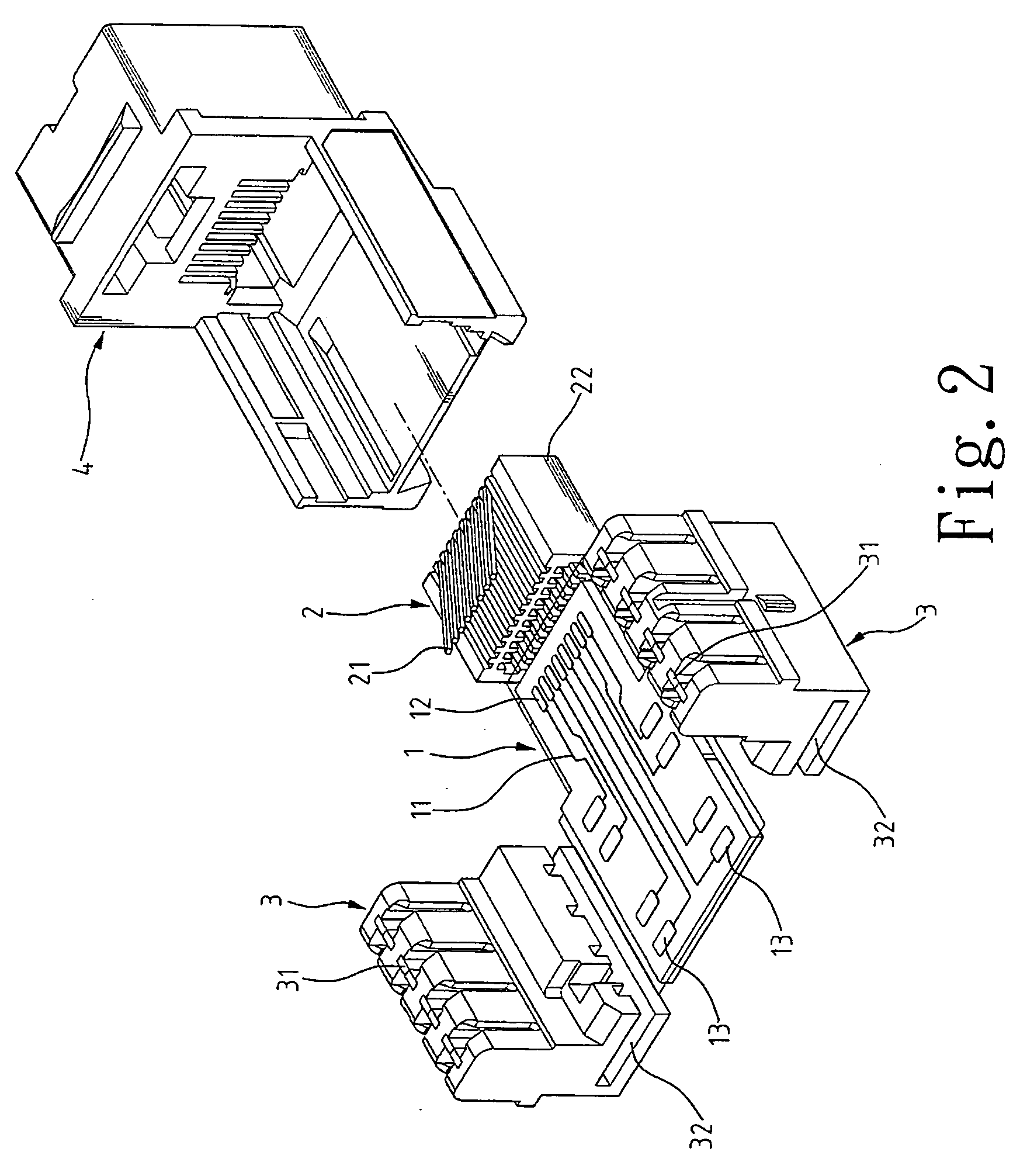
[0027] A preferred embodiment of the present invention will be described in detail with reference to FIG. 1, FIG. 2, FIG. 3 or FIG. 4, an assembled structure of a connector according to the present invention comprises:

[0028] A PCB (1), which has a plurality of wires (11) (act as signal channel), wires (11) form a plurality of jackwire terminals (12) and connector terminals (13) at the front or back of the said PCB in a one-one manner. Moreover, said jackwire terminals (12) and said connector terminals (13) are both formed by metal layer.

[0029] Referring to FIG.3, an I / O port (2) has a plurality of spring jackwires (21) and said spring jackwires (21) correspond to said each jackwire terminal (12) in a one-one manner, each spring jackwire is fixed at the front of a jackwire block (22) respectively so that each spring jackwire (21) is electrically insulated with each other, said jackwire block (22) is hollow and can be embedded in said PCB (1), and each spring jackwire (21) extends d...


PUM


Abstract

The present invention relates to an assembled structure of a connector, which comprises a printed circuit board (PCB), an I / O port, a connector socket configured on a jack frame, wherein spring jackwires in the I / O port and beam contacts in the connector socket form spring plates, so that the spring plates can get a close contact with corresponding terminals and the jackwire block and the connector block can be fixed on the PCB when the jackwire block in the I / O port and the slot in the connector socket joins corresponding terminals on the PCB respectively.

Description

FIELD OF THE INVENTION [0001] The present invention relates to an assembled structure of a connector, particularly to a structure in which the I / O port and connector socket can be connected with the printed circuit board (PCB) fast. BACKGROUND OF THE INVENTION [0002] In traditional connectors, spring jackwires in the I / O port and beam contacts in the connector socket are welded with the PCB to form I / O terminals for signals. Usually, in PCB of such a connector, terminals must cross the PCB to form a through conductive pole in the holes, thus spring jackwires in the I / O port and beam contacts in the connector socket are connected to the PCB in a way of welding or pressing, and such a structure can match wires upon and under the surface of the PCB. SUMMARY OF THE INVENTION [0003] However, in such an assembled structure of said traditional connector, spring jackwires in the I / O port and beam contacts in the connector socket are connected to terminals on the PCB in a way of welding or p...

Claims


Application Information

Patent Timeline
IPC IPC(8): H01R24/00
CPCH01R13/2442H01R24/64H01R13/6658H01R13/502
Inventor WENG, CHING-WEN
Owner PLASTRON PRECISION
Learn More