Flexible package with rigid substrate segments for high density integrated circuit systems

Inactive Publication Date: 2005-06-23
TEXAS INSTR INC
5 Cites 38 Cited by

AI-Extracted Technical Summary

Problems solved by technology

The increase in device complexity, the decrease in feature size, and increase in the number of input/output (I/O) terminals has increased the complexity and difficulty of forming reliable interconnections between the chips and external devices.
As a result of the large size of the substrate, the external contacts experience high levels of mechanical stresses from thermal expansion mismatches between the s...

Method used

[0028]FIG. 2a is a cross sectional view of one embodiment of the invention, including a semiconductor device 20 having multiple rigid substrate segments 21 and 211 attached to a flexible interconnection layer 23. The ability of interconnection layer 23 to flex or to expand and contract between relatively small substrate segments 21 and 211 provides a relief mechanism to minimize thermally induced stresses on external contacts, preferably solder balls 25. In this embodiment, the terminals of semiconductor chip 22, having a large area and/or a high number of I/Os (input/output contacts), are connected to a substrate segment 211, preferably by flip chip bumps 221. The chip supporting substrate segment 211 includes a plurality of conductive vias 212 through which the chip bumps 221 are connected with patterned conductive traces 233 on flexible interconnection layer 23.
[0037] The relatively small, multiple substrates 21,211 interconnected by way of the flexible layer 23 to the solder balls 25 avoids excessively high stresses on the more fragile solder ball interfaces when the device 20 is attached to a PCB (printed circuit board) or other next level of interconnection (not shown). Printed circuit boards (PCB) or other system level interconnections typically are thicker than the device level substrates and are fabricated from a relatively high thermal expansion composite material which imparts stresses on the contacts of semiconductor devices as the system PCB expands and contracts. Stresses on short, rigid solder ball contacts can result in opens or intermittent failures, if the stresses are not relieved. The current invention having a flexible layer between smaller more rigid substrates provides a means for stress relief.
[0043] The flexible interconnection layers 43 and 435 are well suited to a reli...

Benefits of technology

[0017] The stress mitigating assembly of the current invention improves device reliability, performance and i...

Abstract

A reliable, flexible package for high density, high performance, high I/O semiconductor devices including spaced-apart relatively rigid substrate segments mounted on a flexible interconnection layer to mitigate thermally induced stresses. The flexible interconnection layer may further include an integrated ribbon cable connector to provide a secondary system contact.

Application Domain

Technology Topic

Image

  • Flexible package with rigid substrate segments for high density integrated circuit systems
  • Flexible package with rigid substrate segments for high density integrated circuit systems
  • Flexible package with rigid substrate segments for high density integrated circuit systems

Examples

  • Experimental program(1)

Example

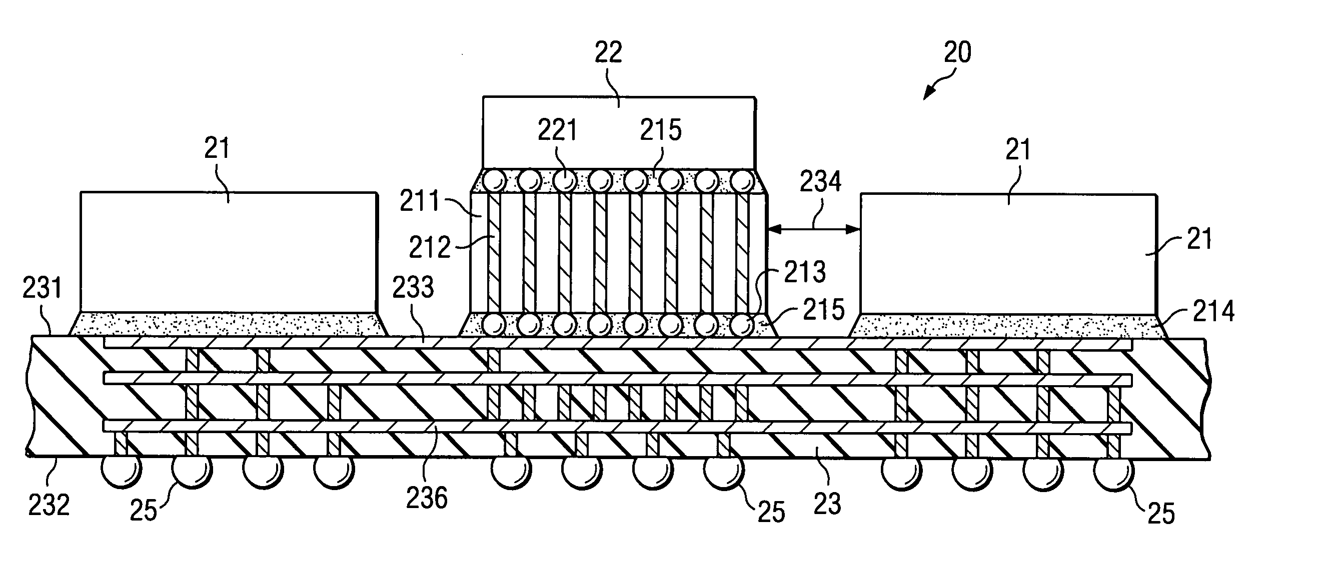
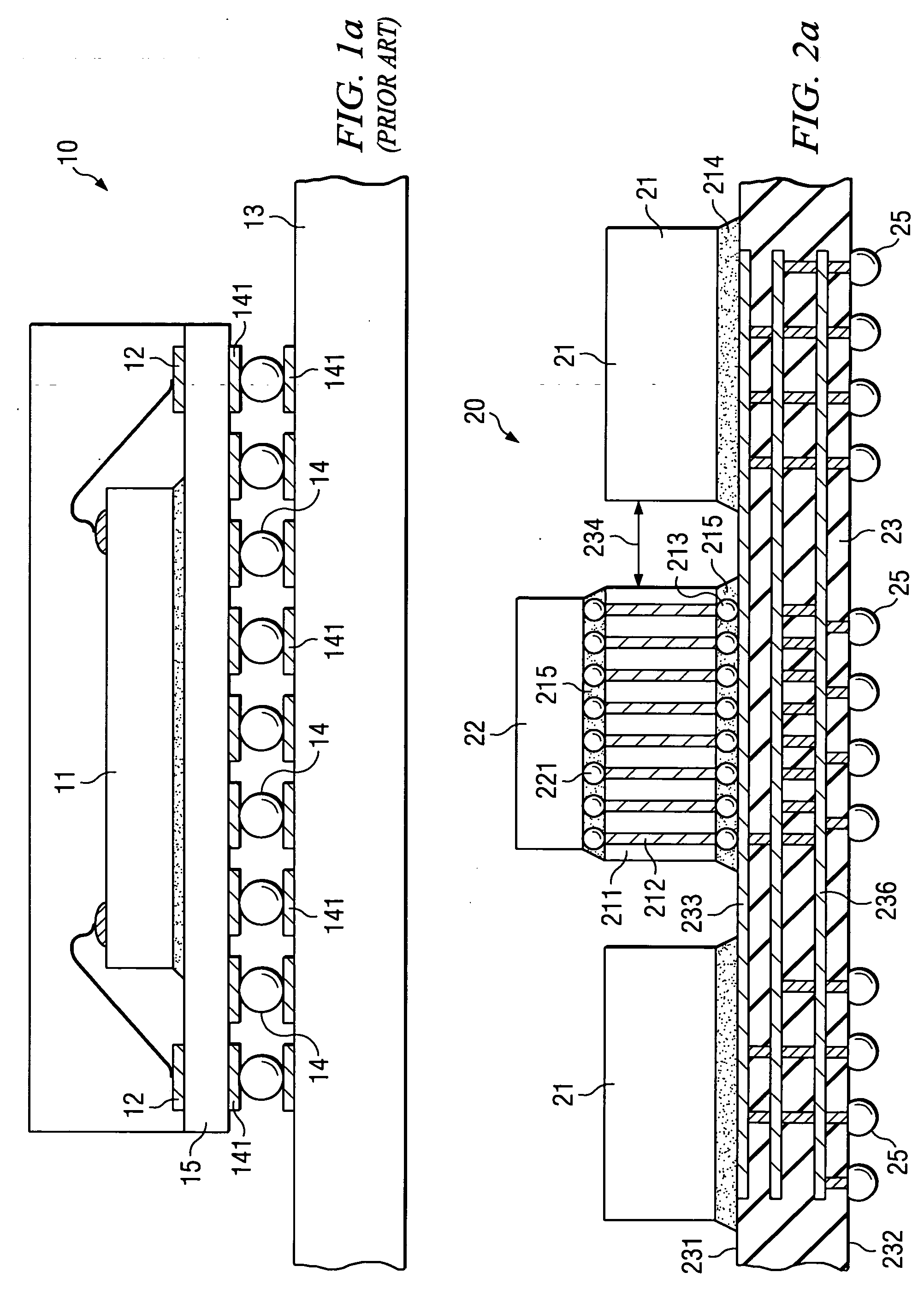
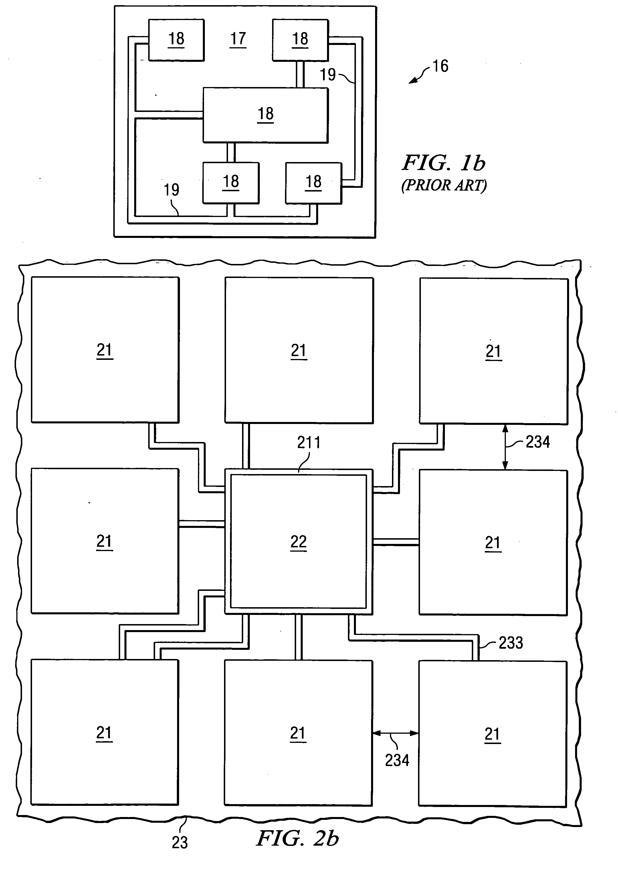
[0038] In a second embodiment of the invention as illustrated in FIG. 3a, device 30 includes semiconductor chip 32 connected to the first surface 331 of flexible interconnection layer 33 and a plurality of substrate segments 31 connected to the second surface of the interconnection layer. Conductive vias 311 through substrate segments 31 provide connection between external solder ball contacts 35 and interconnection layer 33. This second embodiment will be referred to as the “flex-on-top” option.
[0039] Materials of construction for the “flex-on-top” are similar to those in the “flex-on-bottom” option. Chip 32 connections to the first surface 311 of the interconnection layer 31 are preferably flip chip bumps 321, but alternate chip contact techniques such as wire bonding may be used. The flexible interconnection layer 33 comprises a low dielectric polymer with conductive traces 333 providing signal, power and ground connections to substrate segments 31.
[0040] Contacts 312 between the flexible layer 33 and relatively rigid substrate segments 31 may include solder, anisotropic adhesives, or metal coated balls embedded in an adhesive. An underfill material, typically comprising a polymer, may fill the space between contacts 321 and/or 312 to flex layer 33.
[0041] As depicted in FIG. 3b, an embodiment is provided wherein chip 3 and bumps 321 or other interconnections are protected by a preformed cap 37 which may be filled with a polymeric material 38. The cap 37 provides mechanical protection for chip 3 and precludes electrical contact with the back side of the chip. A cap covering the chip is applicable to either the “flex-on-top” or “flex-on-bottom” embodiment.
[0042] Semiconductor devices 20 and 30 depicted in FIGS. 2 and 3 demonstrate single chip embodiments of the invention; however, the assemblage including a multi-segment substrate and flexible interconnection layer is readily adapted to a multi-chip device. FIG. 4a illustrates a “flex-on-top” multi-chip module 4, and device 40 in FIG. 4b is a “flex-on-bottom” embodiment. A circuit having a combination of integrated circuit chips, discrete chips, resistors and/or capacitors may be included in module 4 or module 40, and may be attached by flip chip bump bonding 421, wire bonding 422, or other connection processes.
[0043] The flexible interconnection layers 43 and 435 are well suited to a reliable, high performance multi-chip module embodiment. Conductive planes and traces 431 and 451 comprising patterned thin film metallization within and on the surfaces of flexible dielectric interconnection layers 43 and 435 are readily customized to enhance device performance. For high speed devices having enhanced performance obtained by controlling the impedance of signal paths, the trace widths can be matched, the trace to ground spacing can be controlled, and the ground and power port locations selected in the interconnection layer, thereby providing controlled impedance and reduced reflections.
[0044] The multiple substrate segments of the current invention are superior to large rigid substrates, typical of existing multi-chip modules. The flexible interconnection layer not only allows movement between the segments to avoid high levels of stress on the contacts, but also provides a customized structure for high performance interconnection.
[0045]FIGS. 5a and 5b illustrate yet another embodiment of the invention, including flexible semiconductor device 50 having multiple substrate segments 51 and a flexible interconnection layer 53. External contacts include both solder balls 55 on the second surface of the interconnection layer and an integrated flexible cable 58 for plug-in connection. Cable 58 can be used to plug either I/Os for signal, power or ground into a connector on one portion of a system PCB while the solder balls 55 provide contacts to a second portion of the system. The flexible cable connection coupled with the solder ball contacts to different portions of the system significantly reduces the number of costly layers in a system PCB. Further, flexibility and extension of the ribbon type cable allows latitude in the location of connections, such as a wrap around or to a second PCB.
[0046] Interconnection layer 53 having connections for both solder balls 55 under the device and a ribbon cable connector 58 are applicable to single and multi-chip embodiments, as well as “flex-on-top” or “flex-on-bottom” embodiments. Similarly, the device having only one type of external contacts is applicable to any aforementioned embodiments.
[0047] It will be recognized that a semiconductor device including multiple substrate segments interconnected by a flexible layer is amenable to many modifications which will become apparent to those skilled in the art. Therefore, it is intended that the appended claims be interpreted as broadly as possible.

PUM

no PUM

Description & Claims & Application Information

We can also present the details of the Description, Claims and Application information to help users get a comprehensive understanding of the technical details of the patent, such as background art, summary of invention, brief description of drawings, description of embodiments, and other original content. On the other hand, users can also determine the specific scope of protection of the technology through the list of claims; as well as understand the changes in the life cycle of the technology with the presentation of the patent timeline. Login to view more.

Similar technology patents

Classification and recommendation of technical efficacy words

Why Eureka
Try Eureka